 |
Hilscher netX microcontroller driver
V0.0.5.0
Documentation of the netX driver package
|
|
Hilscher netX microcontroller driver
V0.0.5.0
Documentation of the netX driver package
|
sqi0_app (sqi0_app) More...
#include <netx90_app.h>
Data Fields | |
| union { | |
| __IOM uint32_t sqi_cr0 | |
| struct { | |
| __IOM uint32_t datasize: 4 | |
| __IOM uint32_t bf_align0: 2 | |
| __IOM uint32_t sck_pol: 1 | |
| __IOM uint32_t sck_phase: 1 | |
| __IOM uint32_t sck_muladd: 12 | |
| __IOM uint32_t bf_align1: 2 | |
| __IOM uint32_t sio_cfg: 2 | |
| __IOM uint32_t bf_align2: 3 | |
| __IOM uint32_t filter_in: 1 | |
| __IOM uint32_t bf_align3: 4 | |
| } sqi_cr0_b | |
| }; | |
| union { | |
| __IOM uint32_t sqi_cr1 | |
| struct { | |
| __IOM uint32_t bf_align0: 1 | |
| __IOM uint32_t sqi_en: 1 | |
| __IOM uint32_t bf_align1: 6 | |
| __IOM uint32_t fss: 3 | |
| __IOM uint32_t fss_static: 1 | |
| __IOM uint32_t spi_trans_ctrl: 1 | |
| __IOM uint32_t bf_align2: 3 | |
| __IOM uint32_t tx_fifo_wm: 4 | |
| __IOM uint32_t tx_fifo_clr: 1 | |
| __IOM uint32_t bf_align3: 3 | |
| __IOM uint32_t rx_fifo_wm: 4 | |
| __IOM uint32_t rx_fifo_clr: 1 | |
| __IOM uint32_t bf_align4: 3 | |
| } sqi_cr1_b | |
| }; | |
| union { | |
| __IOM uint32_t sqi_dr | |
| struct { | |
| __IOM uint32_t data: 32 | |
| } sqi_dr_b | |
| }; | |
| union { | |
| __IM uint32_t sqi_sr | |
| struct { | |
| __IM uint32_t tx_fifo_empty: 1 | |
| __IM uint32_t tx_fifo_not_full: 1 | |
| __IM uint32_t rx_fifo_not_empty: 1 | |
| __IM uint32_t rx_fifo_full: 1 | |
| __IM uint32_t busy: 1 | |
| __IM uint32_t bf_align0: 8 | |
| __IM uint32_t sqirom_timeout_err: 1 | |
| __IM uint32_t sqirom_write_err: 1 | |
| __IM uint32_t sqirom_disabled_err: 1 | |
| __IM uint32_t tx_fifo_level: 5 | |
| __IM uint32_t bf_align1: 1 | |
| __IM uint32_t tx_fifo_err_ovfl: 1 | |
| __IM uint32_t tx_fifo_err_undr: 1 | |
| __IM uint32_t rx_fifo_level: 5 | |
| __IM uint32_t bf_align2: 1 | |
| __IM uint32_t rx_fifo_err_ovfl: 1 | |
| __IM uint32_t rx_fifo_err_undr: 1 | |
| } sqi_sr_b | |
| }; | |
| union { | |
| __IOM uint32_t sqi_tcr | |
| struct { | |
| __IOM uint32_t transfer_size: 19 | |
| __IOM uint32_t bf_align0: 2 | |
| __IOM uint32_t tx_out: 1 | |
| __IOM uint32_t tx_oe: 1 | |
| __IOM uint32_t start_transfer: 1 | |
| __IOM uint32_t mode: 2 | |
| __IOM uint32_t duplex: 2 | |
| __IOM uint32_t ms_bit_first: 1 | |
| __IOM uint32_t ms_byte_first: 1 | |
| __IOM uint32_t bf_align1: 2 | |
| } sqi_tcr_b | |
| }; | |
| union { | |
| __IOM uint32_t sqi_irq_mask | |
| struct { | |
| __IOM uint32_t RORIM: 1 | |
| __IOM uint32_t RTIM: 1 | |
| __IOM uint32_t RXIM: 1 | |
| __IOM uint32_t TXIM: 1 | |
| __IOM uint32_t rxneim: 1 | |
| __IOM uint32_t rxfim: 1 | |
| __IOM uint32_t txeim: 1 | |
| __IOM uint32_t trans_end: 1 | |
| __IOM uint32_t sqirom_error: 1 | |
| __IOM uint32_t bf_align0: 23 | |
| } sqi_irq_mask_b | |
| }; | |
| union { | |
| __IOM uint32_t sqi_irq_raw | |
| struct { | |
| __IOM uint32_t RORRIS: 1 | |
| __IOM uint32_t RTRIS: 1 | |
| __IOM uint32_t RXRIS: 1 | |
| __IOM uint32_t TXRIS: 1 | |
| __IOM uint32_t rxneris: 1 | |
| __IOM uint32_t rxfris: 1 | |
| __IOM uint32_t txeris: 1 | |
| __IOM uint32_t trans_end: 1 | |
| __IOM uint32_t sqirom_error: 1 | |
| __IOM uint32_t bf_align0: 23 | |
| } sqi_irq_raw_b | |
| }; | |
| union { | |
| __IM uint32_t sqi_irq_masked | |
| struct { | |
| __IM uint32_t RORMIS: 1 | |
| __IM uint32_t RTMIS: 1 | |
| __IM uint32_t RXMIS: 1 | |
| __IM uint32_t TXMIS: 1 | |
| __IM uint32_t rxnemis: 1 | |
| __IM uint32_t rxfmis: 1 | |
| __IM uint32_t txemis: 1 | |
| __IM uint32_t trans_end: 1 | |
| __IM uint32_t sqirom_error: 1 | |
| __IM uint32_t bf_align0: 23 | |
| } sqi_irq_masked_b | |
| }; | |
| union { | |
| __IOM uint32_t sqi_irq_clear | |
| struct { | |
| __IOM uint32_t RORIC: 1 | |
| __IOM uint32_t RTIC: 1 | |
| __IOM uint32_t RXIC: 1 | |
| __IOM uint32_t TXIC: 1 | |
| __IOM uint32_t rxneic: 1 | |
| __IOM uint32_t rxfic: 1 | |
| __IOM uint32_t txeic: 1 | |
| __IOM uint32_t trans_end: 1 | |
| __IOM uint32_t sqirom_error: 1 | |
| __IOM uint32_t bf_align0: 23 | |
| } sqi_irq_clear_b | |
| }; | |
| union { | |
| __IOM uint32_t sqi_dmacr | |
| struct { | |
| __IOM uint32_t rx_dma_en: 1 | |
| __IOM uint32_t tx_dma_en: 1 | |
| __IOM uint32_t bf_align0: 30 | |
| } sqi_dmacr_b | |
| }; | |
| union { | |
| __IOM uint32_t sqi_pio_out | |
| struct { | |
| __IOM uint32_t sclk: 1 | |
| __IOM uint32_t csn: 3 | |
| __IOM uint32_t mosi: 1 | |
| __IOM uint32_t miso: 1 | |
| __IOM uint32_t sio2: 1 | |
| __IOM uint32_t sio3: 1 | |
| __IOM uint32_t bf_align0: 24 | |
| } sqi_pio_out_b | |
| }; | |
| __IM uint32_t | RESERVED |
| union { | |
| __IOM uint32_t sqi_pio_oe | |
| struct { | |
| __IOM uint32_t sclk: 1 | |
| __IOM uint32_t csn: 3 | |
| __IOM uint32_t mosi: 1 | |
| __IOM uint32_t miso: 1 | |
| __IOM uint32_t sio2: 1 | |
| __IOM uint32_t sio3: 1 | |
| __IOM uint32_t bf_align0: 24 | |
| } sqi_pio_oe_b | |
| }; | |
| union { | |
| __IM uint32_t sqi_pio_in | |
| struct { | |
| __IM uint32_t sclk: 1 | |
| __IM uint32_t csn: 3 | |
| __IM uint32_t mosi: 1 | |
| __IM uint32_t miso: 1 | |
| __IM uint32_t sio2: 1 | |
| __IM uint32_t sio3: 1 | |
| __IM uint32_t bf_align0: 24 | |
| } sqi_pio_in_b | |
| }; | |
| union { | |
| __IOM uint32_t sqi_sqirom_cfg | |
| struct { | |
| __IOM uint32_t enable: 1 | |
| __IOM uint32_t addr_before_cmd: 1 | |
| __IOM uint32_t addr_nibbles: 2 | |
| __IOM uint32_t addr_bits: 3 | |
| __IOM uint32_t bf_align0: 1 | |
| __IOM uint32_t cmd_byte: 8 | |
| __IOM uint32_t dummy_cycles: 4 | |
| __IOM uint32_t t_csh: 2 | |
| __IOM uint32_t bf_align1: 2 | |
| __IOM uint32_t clk_div_val: 8 | |
| } sqi_sqirom_cfg_b | |
| }; | |
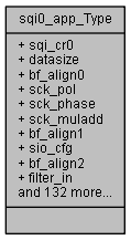
sqi0_app (sqi0_app)
Definition at line 22348 of file netx90_app.h.
| union { ... } |
< (@ 0xFF801180) sqi0_app Structure
| union { ... } |
| union { ... } |
| union { ... } |
| union { ... } |
| union { ... } |
| union { ... } |
| union { ... } |
| union { ... } |
| union { ... } |
| union { ... } |
| union { ... } |
| union { ... } |
| union { ... } |
| __IOM uint32_t sqi0_app_Type::addr_before_cmd |
[1..1] Address before command When set to '1', the address nibbles will be transferred before the command byte. Otherwise, the command will be transferred first (default).
Definition at line 22812 of file netx90_app.h.
| __IOM uint32_t sqi0_app_Type::addr_bits |
[6..4] The number of address bits of the access address considered to generate the address for the SQI chip. This setting depends on the size of the SQI chip. { | 000: 20 bits (1-MByte/8-MBit device) (default) 001: 21 bits (2-MByte/16-MBit device) 010: 22 bits (4-MByte/32-MBit device) 011: 23 bits (8-MByte/64-MBit device) 100: 24 bits (16-MByte/128-MBit device) 101: 25 bits (32-MByte/256-MBit device) 110: 26 bits (64-MByte/512-MBit device) 111: reserved }
Definition at line 22823 of file netx90_app.h.
| __IOM uint32_t sqi0_app_Type::addr_nibbles |
[3..2] The number of nibbles to be transferred as the address to the SQI chip. This setting depends on the command format of the SQI chip. Bit 'addr_before_cmd' controls the address command order. The most significant address bits will be transmitted in the first address nibble. The least significant address bits will be transmitted in the last address nibble. 00: 5 nibbles 01: 6 nibbles (default) 10: 7 nibbles 11: 8 nibbles
Definition at line 22815 of file netx90_app.h.
| __IOM uint32_t sqi0_app_Type::bf_align0 |
[5..4] bitField alignment value for aeabi compatibility
[0..0] bitField alignment value for aeabi compatibility
[20..19] bitField alignment value for aeabi compatibility
[31..9] bitField alignment value for aeabi compatibility
[31..2] bitField alignment value for aeabi compatibility
[31..8] bitField alignment value for aeabi compatibility
[7..7] bitField alignment value for aeabi compatibility
Definition at line 22365 of file netx90_app.h.
| __IM uint32_t sqi0_app_Type::bf_align0 |
[12..5] bitField alignment value for aeabi compatibility
[31..9] bitField alignment value for aeabi compatibility
[31..8] bitField alignment value for aeabi compatibility
Definition at line 22492 of file netx90_app.h.
| __IOM uint32_t sqi0_app_Type::bf_align1 |
[21..20] bitField alignment value for aeabi compatibility
[7..2] bitField alignment value for aeabi compatibility
[31..30] bitField alignment value for aeabi compatibility
[23..22] bitField alignment value for aeabi compatibility
Definition at line 22381 of file netx90_app.h.
| __IM uint32_t sqi0_app_Type::bf_align1 |
[21..21] bitField alignment value for aeabi compatibility
Definition at line 22513 of file netx90_app.h.
| __IOM uint32_t sqi0_app_Type::bf_align2 |
[26..24] bitField alignment value for aeabi compatibility
[15..13] bitField alignment value for aeabi compatibility
Definition at line 22387 of file netx90_app.h.
| __IM uint32_t sqi0_app_Type::bf_align2 |
[29..29] bitField alignment value for aeabi compatibility
Definition at line 22521 of file netx90_app.h.
| __IOM uint32_t sqi0_app_Type::bf_align3 |
[31..28] bitField alignment value for aeabi compatibility
[23..21] bitField alignment value for aeabi compatibility
Definition at line 22397 of file netx90_app.h.
| __IOM uint32_t sqi0_app_Type::bf_align4 |
[31..29] bitField alignment value for aeabi compatibility
Definition at line 22456 of file netx90_app.h.
| __IM uint32_t sqi0_app_Type::busy |
[4..4] Device is busy 1 if data is currently transmitted/received or the transmit FIFO is not empty.
Definition at line 22490 of file netx90_app.h.
| __IOM uint32_t sqi0_app_Type::clk_div_val |
[31..24] clk400 will be divided by (clk_div_val+3) for sqirom_clk generation. Default setting '2' is 80 MHz. Maximum serial clock rate (programming '0') is 133 MHz. Serial clock period (t_sck) will be (clk_div_val+3) * 2.5 ns. Clock high and low phase will be generated symmetrically.
Definition at line 22847 of file netx90_app.h.
| __IOM uint32_t sqi0_app_Type::cmd_byte |
[15..8] This byte is transferred to the SQI chip as the command sequence. Bit 'addr_before_cmd' controls the address command order.
Definition at line 22832 of file netx90_app.h.
| __IOM uint32_t sqi0_app_Type::csn |
[3..1] Chip select/FSS output state {CS2, CS1, CS0}
[3..1] Chip select/FSS output enable {CS2, CS1, CS0}
Definition at line 22744 of file netx90_app.h.
| __IM uint32_t sqi0_app_Type::csn |
[3..1] Chip select/FSS input state {CS2, CS1, CS0}
Definition at line 22779 of file netx90_app.h.
| __IOM uint32_t sqi0_app_Type::data |
[31..0] Transmit data The data must be right-aligned during writing. In Standard SPI mode only bits according to sqi_cr0.datasize are transferred. In SQI mode data must be written in full DWords (i.e. the software has to collect four bytes prior to writing). Unused bytes will not be transferred and may be padded at will (number of transferred bytes depends on sqi_tcr.transfer_size). Receive data will always be right-aligned; unused bits will be '0'.
Definition at line 22470 of file netx90_app.h.
| __IOM uint32_t sqi0_app_Type::datasize |
[3..0] Data size select for standard Motorola SPI mode This bit field is unused in 2-bit and 4-bit SPI modes (i.e. data size fixed to 8 bit). The actual transfer size is 'datasize' + 1 bit. { | 0000...0010: reserved 0011: 4 bit 0100: 5 bit ... 0111: 8 bit ... 1111: 16 bit }
Definition at line 22360 of file netx90_app.h.
| __IOM uint32_t sqi0_app_Type::dummy_cycles |
[19..16] Selects the number of dummy cycles before data will be sampled from the SQI chip. { | 0000: 0 cycles 0001: 1 cycle 0010: 2 cycles (default) ... 1111: 15 cycles }
Definition at line 22835 of file netx90_app.h.
| __IOM uint32_t sqi0_app_Type::duplex |
[27..26] Transfer type selection Default is '11' for standard SPI compatibility. 00: dummy Generates 'transfer_size'
Definition at line 22568 of file netx90_app.h.
| __IOM uint32_t sqi0_app_Type::enable |
[0..0] Enables the SQIROM mode of the SQI module. The SQI chip needs to be initialized to accept 4-bit read-command before you activate the SQIROM mode. This bit is also used to switch between the SQIROM/XiP and the standard SQI/SPI function. If this bit is set, the standard SQI/SPI function is not available. The SQIROM/XiP function does not depend on the programmed value of bit 'sqi_en' of register 'sqi_cr1'. If the multiplex matrix provides the SQI function, it is available only in standard SQI/SPI, but not for
Definition at line 22803 of file netx90_app.h.
| __IOM uint32_t sqi0_app_Type::filter_in |
[27..27] Input filtering Receive data is sampled every 10 ns (100 MHz system clock). If this bit is set, the stored receive value will be the result of a majority decision of the three sampling points around an sck clock edge (if two or more '1's have been sampled, a '1' will be stored. If this bit is not set, a '0' will be stored). Input filtering should be used for sck_muladd<=0x200 (i.e. below 12.5 MHz). For higher frequencies, stable signal phases are too short for filtering.
Definition at line 22388 of file netx90_app.h.
| __IOM uint32_t sqi0_app_Type::fss |
[10..8] Frame slave select Up to 3 devices can be assigned directly. Up to 8 devices can be assigned if an external de-multiplexer is used. This signal is active low, i.e. the bits will be inverted before they are output to the SQI pins.
Definition at line 22416 of file netx90_app.h.
| __IOM uint32_t sqi0_app_Type::fss_static |
[11..11] SQI static chip select 0: Chip select will be generated automatically at data frame begin/end according to fss and datasize. 1: Chip select will be set statically according to 'fss' bits (see below). If fss is set to static mode, fss must be toggled manually after each data frame in Motorola SPI mode when sck_phase is 0 for compatibility with the specification! Note: This bit is used only in standard Motorola SPI mode. For SQI modes, chip select is never generated automatically.
Definition at line 22420 of file netx90_app.h.
| __IOM uint32_t sqi0_app_Type::miso |
[5..5] MISO/SIO1 output state
[5..5] MISO/SIO1 output enable
Definition at line 22746 of file netx90_app.h.
| __IM uint32_t sqi0_app_Type::miso |
[5..5] MISO/SIO1 input state
Definition at line 22781 of file netx90_app.h.
| __IOM uint32_t sqi0_app_Type::mode |
[25..24] SPI/SQI mode selection 00: Standard Motorola SPI mode. 01: 2-bit SPI mode 10: 4-bit SPI mode 11: reserved
Definition at line 22566 of file netx90_app.h.
| __IOM uint32_t sqi0_app_Type::mosi |
[4..4] MOSI/SIO0 output state
[4..4] MOSI/SIO0 output enable
Definition at line 22745 of file netx90_app.h.
| __IM uint32_t sqi0_app_Type::mosi |
[4..4] MOSI/SIO0 input state
Definition at line 22780 of file netx90_app.h.
| __IOM uint32_t sqi0_app_Type::ms_bit_first |
[28..28] Most significant bit first 2- and 4-bit mode: Writing '1' to this bit will transfer most significant bit first (default). In standard Motorola SPI mode this bit is ignored.
Definition at line 22577 of file netx90_app.h.
| __IOM uint32_t sqi0_app_Type::ms_byte_first |
[29..29] Most significant byte first 2- and 4-bit mode: Writing '1' to this bit will use most significant byte first in DWords (big endian). Default is little endian In standard Motorola SPI mode this bit is ignored.
Definition at line 22580 of file netx90_app.h.
| __IM uint32_t sqi0_app_Type::RESERVED |
Definition at line 22752 of file netx90_app.h.
| __IOM uint32_t sqi0_app_Type::RORIC |
[0..0] Clear receive FIFO overrun interrupt
Definition at line 22692 of file netx90_app.h.
| __IOM uint32_t sqi0_app_Type::RORIM |
[0..0] Receive FIFO overrun interrupt mask
Definition at line 22600 of file netx90_app.h.
| __IM uint32_t sqi0_app_Type::RORMIS |
[0..0] Masked receive FIFO overrun interrupt state
Definition at line 22669 of file netx90_app.h.
| __IOM uint32_t sqi0_app_Type::RORRIS |
[0..0] Unmasked receive FIFO overrun interrupt state 1: receive FIFO overrun error occurred 0: no receive FIFO overrun error occurred
Definition at line 22624 of file netx90_app.h.
| __IOM uint32_t sqi0_app_Type::RTIC |
[1..1] Clear receive timeout interrupt
Definition at line 22693 of file netx90_app.h.
| __IOM uint32_t sqi0_app_Type::RTIM |
[1..1] Receive timeout interrupt mask
Definition at line 22601 of file netx90_app.h.
| __IM uint32_t sqi0_app_Type::RTMIS |
[1..1] Masked receive timeout interrupt state
Definition at line 22670 of file netx90_app.h.
| __IOM uint32_t sqi0_app_Type::RTRIS |
[1..1] Unmasked receive timeout interrupt state Timeout period is 32 serial clock periods (depending on adr_sqi_cr0.sck_muladd). 1: receive FIFO is not empty and has not been read out during the timeout period 0: receive FIFO is empty or read during the last timeout period
Definition at line 22627 of file netx90_app.h.
| __IOM uint32_t sqi0_app_Type::rx_dma_en |
[0..0] Enable DMA for SQI-receive data A request will be generated if RX-FIFO is not empty and sqi_cr1.sqi_en (module enable) is set. If the RX-FIFO contains at least 4 words, there will be a burst request to the DMAC. Set dmac_chctrl.SBSize = 1 (i.e. burst size: 4) in the DMAC module. If this bit is reset or the module is disabled, DMA request will also be reset.
Definition at line 22716 of file netx90_app.h.
| __IOM uint32_t sqi0_app_Type::rx_fifo_clr |
[28..28] Receive FIFO clear Writing '1' to this bit will clear the receive FIFO. The hardware will automatically reset this bit. This bit is always '0' when read.
Definition at line 22453 of file netx90_app.h.
| __IM uint32_t sqi0_app_Type::rx_fifo_err_ovfl |
[30..30] Receive FIFO overflow error occurred, data is lost. To clear this status flag, clear RX FIFO (register 'sqi_cr1').
Definition at line 22522 of file netx90_app.h.
| __IM uint32_t sqi0_app_Type::rx_fifo_err_undr |
[31..31] Receive FIFO underrun error has occurred, unexpected data has been read. To clear this status flag, clear RX FIFO (register 'sqi_cr1').
Definition at line 22524 of file netx90_app.h.
| __IM uint32_t sqi0_app_Type::rx_fifo_full |
[3..3] Receive FIFO is full (1 if full).
Definition at line 22489 of file netx90_app.h.
| __IM uint32_t sqi0_app_Type::rx_fifo_level |
[28..24] Receive FIFO level (number of received words to be read from the FIFO).
Definition at line 22519 of file netx90_app.h.
| __IM uint32_t sqi0_app_Type::rx_fifo_not_empty |
[2..2] Receive FIFO is not empty (0 if empty).
Definition at line 22488 of file netx90_app.h.
| __IOM uint32_t sqi0_app_Type::rx_fifo_wm |
[27..24] Receive FIFO watermark for IRQ generation If the receive FIFO watermark IRQ is enabled (bit 'RXIM' is set in register 'sqi_irq_mask'), transfers will stop when the receive FIFO runs full. Transfers will continue after the receive data is read from the receive FIFO to avoid an overflow of the receive FIFO. If the receive FIFO watermark IRQ is disabled (bit 'RXIM' is not set in register 'sqi_irq_mask'), transfers will not stop when the receive FIFO runs full. This may cause an overflow of the receive FIFO. T
Definition at line 22444 of file netx90_app.h.
| __IOM uint32_t sqi0_app_Type::rxfic |
[5..5] Clear receive FIFO full interrupt (for compatibility with netx100/500)
Definition at line 22698 of file netx90_app.h.
| __IOM uint32_t sqi0_app_Type::rxfim |
[5..5] Receive FIFO full interrupt mask (for compatibility with netx100/500)
Definition at line 22606 of file netx90_app.h.
| __IM uint32_t sqi0_app_Type::rxfmis |
[5..5] Masked receive FIFO full interrupt state (for compatibility with netx100/500)
Definition at line 22675 of file netx90_app.h.
| __IOM uint32_t sqi0_app_Type::rxfris |
[5..5] Unmasked receive FIFO full interrupt state (for compatibility with netx100/500) 1: receive FIFO is full 0: receive FIFO is not full
Definition at line 22643 of file netx90_app.h.
| __IOM uint32_t sqi0_app_Type::RXIC |
[2..2] Clear receive FIFO interrupt
Definition at line 22694 of file netx90_app.h.
| __IOM uint32_t sqi0_app_Type::RXIM |
[2..2] Receive FIFO interrupt mask
Definition at line 22602 of file netx90_app.h.
| __IM uint32_t sqi0_app_Type::RXMIS |
[2..2] Masked receive FIFO interrupt state
Definition at line 22671 of file netx90_app.h.
| __IOM uint32_t sqi0_app_Type::rxneic |
[4..4] Clear receive FIFO not empty interrupt (for compatibility with netx100/500)
Definition at line 22696 of file netx90_app.h.
| __IOM uint32_t sqi0_app_Type::rxneim |
[4..4] Receive FIFO not empty interrupt mask (for compatibility with netx100/500)
Definition at line 22604 of file netx90_app.h.
| __IM uint32_t sqi0_app_Type::rxnemis |
[4..4] Masked receive FIFO not empty interrupt state (for compatibility with netx100/500)
Definition at line 22673 of file netx90_app.h.
| __IOM uint32_t sqi0_app_Type::rxneris |
[4..4] Unmasked receive FIFO not empty interrupt state (for compatibility with netx100/500) 1: receive FIFO is not empty 0: receive FIFO is empty
Definition at line 22640 of file netx90_app.h.
| __IOM uint32_t sqi0_app_Type::RXRIS |
[2..2] Unmasked receive FIFO interrupt state 1: receive FIFO is higher than sqi_cr1.rx_fifo_wm 0: receive FIFO is equal or below sqi_cr1.rx_fifo_wm Note: Before programming this IRQ, see description of bits 'spi_trans_ctrl' and 'rx_fifo_wm' of register 'sqi_cr1' for receive FIFO behavior.
Definition at line 22632 of file netx90_app.h.
| __IOM uint32_t sqi0_app_Type::sck_muladd |
[19..8] Serial clock rate multiply add value for sck generation sck-frequency: f_sck = (sck_muladd * 100)/4096 [MHz]. Programmed value of sck_muladd must be <= 0x800. Default value 0x800 equals 50 MHz clock rate. Note: If sck_muladd is set to zero, transfer will freeze. Note: SQIROM (XiP) serial clock rate must be programmed in register 'sqi_sqirom_cfg'.
Definition at line 22375 of file netx90_app.h.
| __IOM uint32_t sqi0_app_Type::sck_phase |
[7..7] Serial clock phase 1: Sample data at second clock edge, data is generated half a clock phase before sampling 0: Sample data at first clock edge, data is generated half a clock phase before sampling Note: sck_phase value equals bit 0 of SPI mode value (mode = (sck_pol, sck_phase)).
Definition at line 22370 of file netx90_app.h.
| __IOM uint32_t sqi0_app_Type::sck_pol |
[6..6] Serial clock polarity 0: idle: clock is low, first edge is rising 1: idle: clock is high, first edge is falling Note: sck_pol value equals bit 1 of SPI mode value (mode = (sck_pol, sck_phase)).
Definition at line 22366 of file netx90_app.h.
| __IOM uint32_t sqi0_app_Type::sclk |
[0..0] Serial SPI clock output state
[0..0] Serial SPI clock output enable
Definition at line 22743 of file netx90_app.h.
| __IM uint32_t sqi0_app_Type::sclk |
[0..0] Serial SPI clock input state
Definition at line 22778 of file netx90_app.h.
| __IOM uint32_t sqi0_app_Type::sio2 |
| __IM uint32_t sqi0_app_Type::sio2 |
[6..6] SIO2 input state
Definition at line 22782 of file netx90_app.h.
| __IOM uint32_t sqi0_app_Type::sio3 |
| __IM uint32_t sqi0_app_Type::sio3 |
[7..7] SIO3 input state
Definition at line 22783 of file netx90_app.h.
| __IOM uint32_t sqi0_app_Type::sio_cfg |
[23..22] SQI IO configuration Default: All additional SQI-IOs (SIO2+3) are in PIO input mode. Coding 00: only SIO2+3 are controllable as PIOs (2-bit SPI or standard Motorola SPI) 01: all SQI IOs are used for transfers (4-bit SPI/SQI) 10: reserved 11: all SQI IOs are controllable as PIOs
Definition at line 22382 of file netx90_app.h.
| __IOM uint32_t sqi0_app_Type::spi_trans_ctrl |
[12..12] Transfer control for standard Motorola SPI (default: disabled) This bit is used only for standard Motorola SPI (bits 'mode' of register 'sqi_tcr') in full-duplex and half-duplex mode. If this bit is set, SPI transfers will be controlled by 'start_transfer' and 'transfer_size' of register 'sqi_tcr'. If this bit is not set (default), SPI transfers start immediately after transfer data has been written to TX FIFO (this is compatible with the SPI module). Settings of 'start_transfer' and 'transfer_size' of reg
Definition at line 22429 of file netx90_app.h.
| __IOM uint32_t sqi0_app_Type::sqi_cr0 |
(@ 0x00000000) SQI control register 0 This register is compatible with the netX50 and netX10 SPI module, but some additional settings are possible. The SQI module provides master function only. Slave settings are omitted. The SQI module does not support the compatible mode for netX100.
Definition at line 22351 of file netx90_app.h.
| struct { ... } sqi0_app_Type::sqi_cr0_b |
| __IOM uint32_t sqi0_app_Type::sqi_cr1 |
(@ 0x00000004) SQI control register 1 This register is compatible with the netX50 and netX10 SPI module, but some additional settings are possible. The SQI module provides master function only. Slave settings are omitted.
Definition at line 22402 of file netx90_app.h.
| struct { ... } sqi0_app_Type::sqi_cr1_b |
| __IOM uint32_t sqi0_app_Type::sqi_dmacr |
(@ 0x00000024) SQI DMA control register This module generates normal transfer requests only (i.e. no last requests will be issued). In consequence, you can use DMAC-controlled transfers only (no peripheral-controlled mode).
Definition at line 22709 of file netx90_app.h.
| struct { ... } sqi0_app_Type::sqi_dmacr_b |
| __IOM uint32_t sqi0_app_Type::sqi_dr |
(@ 0x00000008) SQI data register (DR) Read access: Received data word is delivered from receive FIFO. Write access: Data word to be sent is written to send FIFO. Receive and transmit FIFO both have a depth of 16 words (standard SPI mode). The SQI mode combines both FIFOs, i.e. 64 bytes are available.
Definition at line 22461 of file netx90_app.h.
| struct { ... } sqi0_app_Type::sqi_dr_b |
| __IOM uint32_t sqi0_app_Type::sqi_en |
[1..1] SQI enable 0: Interface disabled 1: Interface enabled Note: If you select the SQIROM/XiP function by bit 'enable' of register 'sqi_sqirom_cfg' (see description of register 'sqi_sqirom_cfg'), the standard SQI/SPI function will not be available.
Definition at line 22410 of file netx90_app.h.
| __IOM uint32_t sqi0_app_Type::sqi_irq_clear |
(@ 0x00000020) SQI interrupt clear register (for compatibility with netX10/50 SPI module). This register is always '0' on read. IRQ flags can also be cleared by writing register 'sqi_irq_raw'.
Definition at line 22686 of file netx90_app.h.
| struct { ... } sqi0_app_Type::sqi_irq_clear_b |
| __IOM uint32_t sqi0_app_Type::sqi_irq_mask |
(@ 0x00000014) SQI interrupt mask register: IRQ mask is an AND-mask: Only raw interrupts with mask bit set can generate a module IRQ to CPU. For detailed IRQ behavior and function, see register 'sqi_irq_raw'. The functionality of this register is similar to that of the corresponding SPI register spi_imsc. In contrast to this register, setting bits in spi_imsc also clears the corresponding raw interrupts.
Definition at line 22589 of file netx90_app.h.
| struct { ... } sqi0_app_Type::sqi_irq_mask_b |
| __IM uint32_t sqi0_app_Type::sqi_irq_masked |
(@ 0x0000001C) SQI masked interrupt status register For detailed IRQ behavior and function, see register 'sqi_irq_raw'.
Definition at line 22664 of file netx90_app.h.
| struct { ... } sqi0_app_Type::sqi_irq_masked_b |
| __IOM uint32_t sqi0_app_Type::sqi_irq_raw |
(@ 0x00000018) SQI interrupt state before masking register (raw interrupt). Writing a '1' to a bit clears this interrupt. IRQ flags can also be cleared by using 'sqi_irq_clear' for SPI module compatibility.
Definition at line 22617 of file netx90_app.h.
| struct { ... } sqi0_app_Type::sqi_irq_raw_b |
| __IM uint32_t sqi0_app_Type::sqi_pio_in |
(@ 0x00000034) SQI PIO input status register Bits 'sio_cfg' of register 'sqi_cr0' control the IO PIO mode.
Definition at line 22773 of file netx90_app.h.
| struct { ... } sqi0_app_Type::sqi_pio_in_b |
| __IOM uint32_t sqi0_app_Type::sqi_pio_oe |
(@ 0x00000030) SQI PIO output enable control register Bits 'sio_cfg' of register 'sqi_cr0' control the IO PIO mode. Bit 'sqi_en' of register 'sqi_cr0' has to be set to drive the SQI IOs in the PIO mode.
Definition at line 22755 of file netx90_app.h.
| struct { ... } sqi0_app_Type::sqi_pio_oe_b |
| __IOM uint32_t sqi0_app_Type::sqi_pio_out |
(@ 0x00000028) SQI PIO output level control register Bits 'sio_cfg' of register 'sqi_cr0' control the IO PIO mode. Bit 'sqi_en' of register 'sqi_cr0' has to be set to drive the SQI IOs in the PIO mode. PIO input signal states are never filtered (bit 'filter_in' of register 'sqi_cr0').
Definition at line 22735 of file netx90_app.h.
| struct { ... } sqi0_app_Type::sqi_pio_out_b |
| __IOM uint32_t sqi0_app_Type::sqi_sqirom_cfg |
(@ 0x00000038) SQIROM mode configuration This mode supports the 'eXecute in Place' (XiP) feature of SQI flash chips. This register serves to configure the position of command byte and address nibbles as well as the number of address nibbles and dummy cycles. To support a wide range of frequencies for the serial clock output, you can also change the clock divider. Notes: 1. Before enabling this mode, make sure that the SQI flash chip is in 4-bit command mode, otherwise the module is not able to fetch da
Definition at line 22789 of file netx90_app.h.
| struct { ... } sqi0_app_Type::sqi_sqirom_cfg_b |
| __IM uint32_t sqi0_app_Type::sqi_sr |
(@ 0x0000000C) Read-only SQI status register Shows the current status of the SQI interface.
Definition at line 22482 of file netx90_app.h.
| struct { ... } sqi0_app_Type::sqi_sr_b |
| __IOM uint32_t sqi0_app_Type::sqi_tcr |
(@ 0x00000010) SQI transfer control This register must not be changed during a transfer (bit 'busy' of register 'sqi_sr' is '1') to avoid corrupted transfers causing damage to the hardware. Module address offset 0x10 is reserved in the netX10/50 SPI module. Thus, no compatibility problems will result from using this address for extended transfer control features.
Definition at line 22531 of file netx90_app.h.
| struct { ... } sqi0_app_Type::sqi_tcr_b |
| __IM uint32_t sqi0_app_Type::sqirom_disabled_err |
[15..15] Access to the disabled SQIROM area has occurred. To enable the SQIROM function, set bit 'enable' in register 'sqi_sqirom_cfg'. This bit can be used to determine why the IRQ 'sqirom_error' has occurred. Clearing this status flag is possible only by writing a '1' here.
Definition at line 22506 of file netx90_app.h.
| __IOM uint32_t sqi0_app_Type::sqirom_error |
[8..8] SQIROM error interrupt mask
[8..8] Unmasked SQIROM error interrupt state 1: SQIROM access error detected. This IRQ will be set if an error occurs during an SQIROM access. For detailed information on the error, see SQIROM error bits in register 'sqi_sr'. For error handling, clear this IRQ bit and the bits of register 'sqi_sr'. 0: no SQIROM error detected.
[8..8] Clear SQIROM error interrupt
Definition at line 22611 of file netx90_app.h.
| __IM uint32_t sqi0_app_Type::sqirom_error |
[8..8] Masked SQIROM error interrupt state
Definition at line 22680 of file netx90_app.h.
| __IM uint32_t sqi0_app_Type::sqirom_timeout_err |
[13..13] Timeout during a read of the SQIROM area has occurred. A timeout results from a fix level of the netX serial clock IO. Check IO multiplexing configuration and make sure that the serial clock output is not externally clamped. This bit can be used to determine why the IRQ 'sqirom_error' has occurred. Clearing this status flag is possible only by writing a '1' here. The SQIROM function must be disabled and enabled again to reset module-internal state machines after this bit has been set (register 'sqirom_cfg'
Definition at line 22493 of file netx90_app.h.
| __IM uint32_t sqi0_app_Type::sqirom_write_err |
[14..14] Write access to the read-only SQIROM area has occurred. This bit can be used to determine why the IRQ 'sqirom_error' has occurred. Clearing this status flag is possible only by writing a '1' here.
Definition at line 22502 of file netx90_app.h.
| __IOM uint32_t sqi0_app_Type::start_transfer |
[23..23] Transfer start signal Writing a '1' starts the transfer of transfer_size bytes or dummy cycles. The hardware will automatically reset this bit. This bit is always '0' when read. This bit is writable only after a transfer sequence is finished or if it has been terminated by a FIFO clear. Note: A transfer sequence is finished completely when 'busy' of register 'sqi_sr' is not set. Note: In standard Motorola SPI mode, this function can be controlled by bit 'spi_trans_ctrl' of register 'sqi_cr1' (for SPI modul
Definition at line 22557 of file netx90_app.h.
| __IOM uint32_t sqi0_app_Type::t_csh |
[21..20] Min. SQI chip select high (idle) time: (t_csh+1) * t_sck (according to clk_div_val). Programmable values are 0 to 3. Change this parameter if the SQI device used requires min. chip select high times exceeding 1 serial clock period. The data sheet of the SQI device used provides the required timing. Note: Serial clock will not toggle if the device is not selected. Hence, only chip select active timing has to be considered.
Definition at line 22838 of file netx90_app.h.
| __IOM uint32_t sqi0_app_Type::trans_end |
[7..7] Transfer end interrupt mask
[7..7] Unmasked transfer end interrupt state (related to bit 'busy' of register 'sqi_sr') 1: transfer finished. Bit 'busy' of register 'sqi_sr' has become inactive. 0: transfer not finished. Bit 'busy' of register 'sqi_sr' is active.
[7..7] Clear transfer end interrupt
Definition at line 22610 of file netx90_app.h.
| __IM uint32_t sqi0_app_Type::trans_end |
[7..7] Masked transfer end interrupt state
Definition at line 22679 of file netx90_app.h.
| __IOM uint32_t sqi0_app_Type::transfer_size |
[18..0] Number of bytes within the current SQI transaction Program (number of bytes - 1) or (number of dummy clock cycles
Definition at line 22541 of file netx90_app.h.
| __IOM uint32_t sqi0_app_Type::tx_dma_en |
[1..1] Enable DMA for SQI-transmit data A request will be generated if TX-FIFO is not full and sqi_cr1.sqi_en (module enable) is set. If at least 4 words are writable to the TX-FIFO, there will be a burst request to the DMAC. Set dmac_chctrl.DBSize = 1 (i.e. burst size: 4) in the DMAC module. If this bit is reset or the module is disabled, DMA request will also be reset.
Definition at line 22723 of file netx90_app.h.
| __IOM uint32_t sqi0_app_Type::tx_fifo_clr |
[20..20] Transmit FIFO clear Writing '1' to this bit will clear the transmit FIFO. The hardware will automatically reset this bit. This bit is always '0' when read.
Definition at line 22440 of file netx90_app.h.
| __IM uint32_t sqi0_app_Type::tx_fifo_empty |
[0..0] Transmit FIFO is empty (1 if empty).
Definition at line 22486 of file netx90_app.h.
| __IM uint32_t sqi0_app_Type::tx_fifo_err_ovfl |
[22..22] Transmit FIFO overflow error occurred, data is lost. To clear this status flag, clear TX FIFO (register 'sqi_cr1').
Definition at line 22514 of file netx90_app.h.
| __IM uint32_t sqi0_app_Type::tx_fifo_err_undr |
[23..23] Transmit FIFO underrun error has occurred, unexpected data has been sent. To clear this status flag, clear TX FIFO (register 'sqi_cr1').
Definition at line 22516 of file netx90_app.h.
| __IM uint32_t sqi0_app_Type::tx_fifo_level |
[20..16] Transmit FIFO level (number of words to be transmitted are left in the FIFO).
Definition at line 22511 of file netx90_app.h.
| __IM uint32_t sqi0_app_Type::tx_fifo_not_full |
[1..1] Transmit FIFO is not full (0 if full).
Definition at line 22487 of file netx90_app.h.
| __IOM uint32_t sqi0_app_Type::tx_fifo_wm |
[19..16] Transmit FIFO watermark for IRQ generation
Definition at line 22439 of file netx90_app.h.
| __IOM uint32_t sqi0_app_Type::tx_oe |
[22..22] Output driver enable in dummy or standard SPI receive-only mode Writing a '1' enables the output drivers of the data pins in the dummy mode.
Definition at line 22554 of file netx90_app.h.
| __IOM uint32_t sqi0_app_Type::tx_out |
[21..21] Output level in dummy or standard SPI receive-only mode This bit selects the output level when the output driver is enabled in the dummy mode.
Definition at line 22551 of file netx90_app.h.
| __IOM uint32_t sqi0_app_Type::txeic |
[6..6] Clear transmit FIFO empty interrupt (for compatibility with netx100/500)
Definition at line 22700 of file netx90_app.h.
| __IOM uint32_t sqi0_app_Type::txeim |
[6..6] Transmit FIFO empty interrupt mask (for compatibility with netx100/500)
Definition at line 22608 of file netx90_app.h.
| __IM uint32_t sqi0_app_Type::txemis |
[6..6] Masked transmit FIFO empty interrupt state (for compatibility with netx100/500)
Definition at line 22677 of file netx90_app.h.
| __IOM uint32_t sqi0_app_Type::txeris |
[6..6] Unmasked transmit FIFO empty interrupt state (for compatibility with netx100/500) 1: transmit FIFO is empty 0: transmit FIFO is not empty
Definition at line 22646 of file netx90_app.h.
| __IOM uint32_t sqi0_app_Type::TXIC |
[3..3] Clear transmit FIFO interrupt
Definition at line 22695 of file netx90_app.h.
| __IOM uint32_t sqi0_app_Type::TXIM |
[3..3] Transmit FIFO interrupt mask
Definition at line 22603 of file netx90_app.h.
| __IM uint32_t sqi0_app_Type::TXMIS |
[3..3] Masked transmit FIFO interrupt state
Definition at line 22672 of file netx90_app.h.
| __IOM uint32_t sqi0_app_Type::TXRIS |
[3..3] Unmasked transmit FIFO interrupt state 1: transmit FIFO level is below sqi_cr1.tx_fifo_wm 0: transmit FIFO is equal or higher than sqi_cr1.tx_fifo_wm
Definition at line 22637 of file netx90_app.h.
 1.8.11