 |
Hilscher netX microcontroller driver
V0.0.5.0
Documentation of the netX driver package
|
|
Hilscher netX microcontroller driver
V0.0.5.0
Documentation of the netX driver package
|
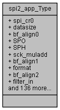
spi2_app (spi2_app) More...
#include <netx90_app.h>
Data Fields | |
| union { | |
| __IOM uint32_t spi_cr0 | |
| struct { | |
| __IOM uint32_t datasize: 4 | |
| __IOM uint32_t bf_align0: 2 | |
| __IOM uint32_t SPO: 1 | |
| __IOM uint32_t SPH: 1 | |
| __IOM uint32_t sck_muladd: 12 | |
| __IOM uint32_t bf_align1: 4 | |
| __IOM uint32_t format: 2 | |
| __IOM uint32_t bf_align2: 1 | |
| __IOM uint32_t filter_in: 1 | |
| __IOM uint32_t slave_sig_early: 1 | |
| __IOM uint32_t bf_align3: 2 | |
| __IOM uint32_t netx100_comp: 1 | |
| } spi_cr0_b | |
| }; | |
| union { | |
| __IOM uint32_t spi_cr1 | |
| struct { | |
| __IOM uint32_t LBM: 1 | |
| __IOM uint32_t SSE: 1 | |
| __IOM uint32_t MS: 1 | |
| __IOM uint32_t SOD: 1 | |
| __IOM uint32_t bf_align0: 4 | |
| __IOM uint32_t fss: 3 | |
| __IOM uint32_t fss_static: 1 | |
| __IOM uint32_t bf_align1: 4 | |
| __IOM uint32_t tx_fifo_wm: 4 | |
| __IOM uint32_t tx_fifo_clr: 1 | |
| __IOM uint32_t bf_align2: 3 | |
| __IOM uint32_t rx_fifo_wm: 4 | |
| __IOM uint32_t rx_fifo_clr: 1 | |
| __IOM uint32_t bf_align3: 3 | |
| } spi_cr1_b | |
| }; | |
| union { | |
| __IOM uint32_t spi_dr | |
| struct { | |
| __IOM uint32_t data: 17 | |
| __IOM uint32_t bf_align0: 15 | |
| } spi_dr_b | |
| }; | |
| union { | |
| __IM uint32_t spi_sr | |
| struct { | |
| __IM uint32_t TFE: 1 | |
| __IM uint32_t TNF: 1 | |
| __IM uint32_t RNE: 1 | |
| __IM uint32_t RFF: 1 | |
| __IM uint32_t BSY: 1 | |
| __IM uint32_t bf_align0: 11 | |
| __IM uint32_t tx_fifo_level: 5 | |
| __IM uint32_t bf_align1: 1 | |
| __IM uint32_t tx_fifo_err_ovfl: 1 | |
| __IM uint32_t tx_fifo_err_undr: 1 | |
| __IM uint32_t rx_fifo_level: 5 | |
| __IM uint32_t bf_align2: 1 | |
| __IM uint32_t rx_fifo_err_ovfl: 1 | |
| __IM uint32_t rx_fifo_err_undr: 1 | |
| } spi_sr_b | |
| }; | |
| __IM uint32_t | RESERVED |
| union { | |
| __IOM uint32_t spi_imsc | |
| struct { | |
| __IOM uint32_t RORIM: 1 | |
| __IOM uint32_t RTIM: 1 | |
| __IOM uint32_t RXIM: 1 | |
| __IOM uint32_t TXIM: 1 | |
| __IOM uint32_t rxneim: 1 | |
| __IOM uint32_t rxfim: 1 | |
| __IOM uint32_t txeim: 1 | |
| __IOM uint32_t bf_align0: 25 | |
| } spi_imsc_b | |
| }; | |
| union { | |
| __IM uint32_t spi_ris | |
| struct { | |
| __IM uint32_t RORRIS: 1 | |
| __IM uint32_t RTRIS: 1 | |
| __IM uint32_t RXRIS: 1 | |
| __IM uint32_t TXRIS: 1 | |
| __IM uint32_t rxneris: 1 | |
| __IM uint32_t rxfris: 1 | |
| __IM uint32_t txeris: 1 | |
| __IM uint32_t bf_align0: 25 | |
| } spi_ris_b | |
| }; | |
| union { | |
| __IM uint32_t spi_mis | |
| struct { | |
| __IM uint32_t RORMIS: 1 | |
| __IM uint32_t RTMIS: 1 | |
| __IM uint32_t RXMIS: 1 | |
| __IM uint32_t TXMIS: 1 | |
| __IM uint32_t rxnemis: 1 | |
| __IM uint32_t rxfmis: 1 | |
| __IM uint32_t txemis: 1 | |
| __IM uint32_t bf_align0: 25 | |
| } spi_mis_b | |
| }; | |
| union { | |
| __IOM uint32_t spi_icr | |
| struct { | |
| __IOM uint32_t RORIC: 1 | |
| __IOM uint32_t RTIC: 1 | |
| __IOM uint32_t RXIC: 1 | |
| __IOM uint32_t TXIC: 1 | |
| __IOM uint32_t rxneic: 1 | |
| __IOM uint32_t rxfic: 1 | |
| __IOM uint32_t txeic: 1 | |
| __IOM uint32_t bf_align0: 25 | |
| } spi_icr_b | |
| }; | |
| __IM uint32_t | RESERVED1 |
| union { | |
| __IOM uint32_t spi_dmacr | |
| struct { | |
| __IOM uint32_t RXDMAE: 1 | |
| __IOM uint32_t TXDMAE: 1 | |
| __IOM uint32_t bf_align0: 30 | |
| } spi_dmacr_b | |
| }; | |
| __IM uint32_t | RESERVED2 |
| union { | |
| __IOM uint32_t spi_data_register | |
| struct { | |
| __IOM uint32_t data_byte_0: 8 | |
| __IOM uint32_t data_byte_1: 8 | |
| __IOM uint32_t dr_valid0: 1 | |
| __IOM uint32_t dr_valid1: 1 | |
| __IOM uint32_t bf_align0: 14 | |
| } spi_data_register_b | |
| }; | |
| union { | |
| __IM uint32_t spi_status_register | |
| struct { | |
| __IM uint32_t SR_in_fuel_val: 9 | |
| __IM uint32_t SR_out_fuel_val: 9 | |
| __IM uint32_t SR_in_fuel: 1 | |
| __IM uint32_t SR_in_recdata: 1 | |
| __IM uint32_t SR_in_full: 1 | |
| __IM uint32_t SR_out_fuel: 1 | |
| __IM uint32_t SR_out_fw: 1 | |
| __IM uint32_t SR_out_empty: 1 | |
| __IM uint32_t SR_out_full: 1 | |
| __IM uint32_t SR_selected: 1 | |
| __IM uint32_t bf_align0: 6 | |
| } spi_status_register_b | |
| }; | |
| union { | |
| __IOM uint32_t spi_control_register | |
| struct { | |
| __IOM uint32_t CR_softreset: 1 | |
| __IOM uint32_t CR_speed: 4 | |
| __IOM uint32_t bf_align0: 1 | |
| __IOM uint32_t CR_read: 1 | |
| __IOM uint32_t CR_write: 1 | |
| __IOM uint32_t CR_ss: 3 | |
| __IOM uint32_t CS_mode: 1 | |
| __IOM uint32_t bf_align1: 8 | |
| __IOM uint32_t CR_clr_infifo: 1 | |
| __IOM uint32_t CR_clr_outfifo: 1 | |
| __IOM uint32_t CR_burstdelay: 3 | |
| __IOM uint32_t CR_burst: 3 | |
| __IOM uint32_t CR_ncpha: 1 | |
| __IOM uint32_t CR_cpol: 1 | |
| __IOM uint32_t CR_ms: 1 | |
| __IOM uint32_t CR_en: 1 | |
| } spi_control_register_b | |
| }; | |
| union { | |
| __IOM uint32_t spi_interrupt_control_register | |
| struct { | |
| __IOM uint32_t IR_in_fuel: 9 | |
| __IOM uint32_t IR_out_fuel: 9 | |
| __IOM uint32_t IR_in_fuel_en: 1 | |
| __IOM uint32_t IR_in_recdata_en: 1 | |
| __IOM uint32_t IR_in_full_en: 1 | |
| __IOM uint32_t IR_out_fuel_en: 1 | |
| __IOM uint32_t IR_out_fw_en: 1 | |
| __IOM uint32_t IR_out_empty_en: 1 | |
| __IOM uint32_t IR_out_full_en: 1 | |
| __IOM uint32_t bf_align0: 7 | |
| } spi_interrupt_control_register_b | |
| }; | |
spi2_app (spi2_app)
Definition at line 21915 of file netx90_app.h.
| union { ... } |
< (@ 0xFF801140) spi2_app Structure
| union { ... } |
| union { ... } |
| union { ... } |
| union { ... } |
| union { ... } |
| union { ... } |
| union { ... } |
| union { ... } |
| union { ... } |
| union { ... } |
| union { ... } |
| union { ... } |
| __IOM uint32_t spi2_app_Type::bf_align0 |
[5..4] bitField alignment value for aeabi compatibility
[7..4] bitField alignment value for aeabi compatibility
[31..17] bitField alignment value for aeabi compatibility
[31..7] bitField alignment value for aeabi compatibility
[31..2] bitField alignment value for aeabi compatibility
[31..18] bitField alignment value for aeabi compatibility
[5..5] bitField alignment value for aeabi compatibility
[31..25] bitField alignment value for aeabi compatibility
Definition at line 21927 of file netx90_app.h.
| __IM uint32_t spi2_app_Type::bf_align0 |
[15..5] bitField alignment value for aeabi compatibility
[31..7] bitField alignment value for aeabi compatibility
[31..26] bitField alignment value for aeabi compatibility
Definition at line 22057 of file netx90_app.h.
| __IOM uint32_t spi2_app_Type::bf_align1 |
[23..20] bitField alignment value for aeabi compatibility
[15..12] bitField alignment value for aeabi compatibility
[19..12] bitField alignment value for aeabi compatibility
Definition at line 21944 of file netx90_app.h.
| __IM uint32_t spi2_app_Type::bf_align1 |
[21..21] bitField alignment value for aeabi compatibility
Definition at line 22060 of file netx90_app.h.
| __IOM uint32_t spi2_app_Type::bf_align2 |
[26..26] bitField alignment value for aeabi compatibility
[23..21] bitField alignment value for aeabi compatibility
Definition at line 21947 of file netx90_app.h.
| __IM uint32_t spi2_app_Type::bf_align2 |
[29..29] bitField alignment value for aeabi compatibility
Definition at line 22065 of file netx90_app.h.
| __IOM uint32_t spi2_app_Type::bf_align3 |
[30..29] bitField alignment value for aeabi compatibility
[31..29] bitField alignment value for aeabi compatibility
Definition at line 21965 of file netx90_app.h.
| __IM uint32_t spi2_app_Type::BSY |
[4..4] Device busy (1 if data is currently transmitted/received or the transmit FIFO is not empty)
Definition at line 22055 of file netx90_app.h.
| __IOM uint32_t spi2_app_Type::CR_burst |
[27..25] netx100/netx500 only, obsolete in later versions: burst length = 2^CR_burst
Definition at line 22293 of file netx90_app.h.
| __IOM uint32_t spi2_app_Type::CR_burstdelay |
[24..22] netx100/netx500 only, obsolete in later versions: delay between transmission of 2 data bytes (0 to 7 SCK cycles)
Definition at line 22291 of file netx90_app.h.
| __IOM uint32_t spi2_app_Type::CR_clr_infifo |
[20..20] Clear input FIFO
Definition at line 22289 of file netx90_app.h.
| __IOM uint32_t spi2_app_Type::CR_clr_outfifo |
[21..21] Clear output FIFO
Definition at line 22290 of file netx90_app.h.
| __IOM uint32_t spi2_app_Type::CR_cpol |
[29..29] 1: falling edge of SCK is primary 0: rising edge of SCK is primary
Definition at line 22300 of file netx90_app.h.
| __IOM uint32_t spi2_app_Type::CR_en |
[31..31] 1: enable 0: disable SPI interface
Definition at line 22303 of file netx90_app.h.
| __IOM uint32_t spi2_app_Type::CR_ms |
[30..30] 1: master mode 0:slave mode
Definition at line 22302 of file netx90_app.h.
| __IOM uint32_t spi2_app_Type::CR_ncpha |
[28..28] SPI clock phase mode (Note: meaning of this bit is inverted to functionality of bit spi_cr0.SPH): { | 0: change data on secondary SCK edge data is active on primary SCK edge 1: change data on primary SCK edge data is active on secondary SCK edge }
Definition at line 22295 of file netx90_app.h.
| __IOM uint32_t spi2_app_Type::CR_read |
[6..6] netx100/netx500 only, in later versions always '1': 1: enable SPI interface read data
Definition at line 22280 of file netx90_app.h.
| __IOM uint32_t spi2_app_Type::CR_softreset |
[0..0] write only: no function in netx100/netx500; later versions: clears IRQs and FIFOs
Definition at line 22268 of file netx90_app.h.
| __IOM uint32_t spi2_app_Type::CR_speed |
[4..1] Clock divider for SPI clock (2 - 2^16) If SPI clock rate is changed using spi_cr0.sck_muladd, this value will not be updated and may be incorrect There are 16 different SPI clocks frequencies to choose: 0000: 0.025 MHz (Note: Not compatible to netx100/500. '0000' freezes SCK in netx100/500.) 0001: 0.05 MHz 0010: 0.1 MHz 0011: 0.2 MHz 0100: 0.5 MHz 0101: 1 MHz 0110: 1.25 MHz 0111: 2 MHz 1000: 2.5 MHz 1001: 3.3333 MHz 1010: 5 MHz 1011: 10 MHz 1100: 12.5 MHz 1101: 16.6666 MHz 1110: 25 MHz 1111: 50 MHz
Definition at line 22270 of file netx90_app.h.
| __IOM uint32_t spi2_app_Type::CR_ss |
[10..8] External slave select
Definition at line 22284 of file netx90_app.h.
| __IOM uint32_t spi2_app_Type::CR_write |
[7..7] netx100/netx500 only, in later versions always '1': 1: enable SPI interface write data
Definition at line 22282 of file netx90_app.h.
| __IOM uint32_t spi2_app_Type::CS_mode |
[11..11] 1: chip select is generated automatically by the internal state machine 0: chip select is directly controlled by software (see bits CR_ss).
Definition at line 22285 of file netx90_app.h.
| __IOM uint32_t spi2_app_Type::data |
[16..0] Transmit data: Only lowest bits according to spi_cr0.datasize will be sent. Receive data will be delivered on the lowest bits, unused bits (above spi_cr0.datasize) will be '0'. In slave mode transmit data is requested from the FIFO when the last bit of the currently transferred word is set to the MISO signal. If no next transmit data can be read from the FIFO until the current word's last bit was transferred, a FIFO underrun will occur in case chip-select does not go inactive at the next detected SCK edge.
Definition at line 22030 of file netx90_app.h.
| __IOM uint32_t spi2_app_Type::data_byte_0 |
[7..0] Data byte 0
Definition at line 22220 of file netx90_app.h.
| __IOM uint32_t spi2_app_Type::data_byte_1 |
[15..8] Obsolete, don't use
Definition at line 22221 of file netx90_app.h.
| __IOM uint32_t spi2_app_Type::datasize |
[3..0] DSS: data size select (transfer size = datasize + 1 bits): { | 0000...0010: reserved 0011: 4 bit 0100: 5 bit ... 0111: 8 bit ... 1111: 16 bit } Note: 16 bit TX-data-loss bug of netX50/netX5 is fixed since netX10.
Definition at line 21923 of file netx90_app.h.
| __IOM uint32_t spi2_app_Type::dr_valid0 |
[16..16] Valid bit for data_byte_0 This bit shows if data_byte_0 is valid and must be set during a FIFO write access.
Definition at line 22222 of file netx90_app.h.
| __IOM uint32_t spi2_app_Type::dr_valid1 |
[17..17] Obsolete, always 0
Definition at line 22224 of file netx90_app.h.
| __IOM uint32_t spi2_app_Type::filter_in |
[27..27] Receive data is sampled every 10ns (100MHz system clock). If this bit is set, the stored receive value will be the result of a majority decision of the three sampling points around a SPI-clock edge (if two or more '1s! were sampled a '1' will be stored, else a '0' will be stored. In slave mode chip-select and SCK edges will also be detected by oversampling if this bit is set: An edge will be detected if the majority-result of 3 subsequent sampled values toggles. Input filtering should be used for sck_mulad
Definition at line 21948 of file netx90_app.h.
| __IOM uint32_t spi2_app_Type::format |
[25..24] Frame format: 00: Motorola SPI frame format 01..11: reserved
Definition at line 21945 of file netx90_app.h.
| __IOM uint32_t spi2_app_Type::fss |
[10..8] Frame or slave select. There are up to 3 external SPI chip-select signals. In master mode, the fss bits define the states of the chip-select signals. The inversion for low-active chip-selects (e.g. for Motorola SPI frame format) is done automatically depending on the value programmed to the 'format' bits. Example: To use the netX IO CS1 as chip-select, program '010' here, regardless whether the external chip-select is low or high active. In slave mode, the fss bits are a mask to select which netX input sho
Definition at line 21988 of file netx90_app.h.
| __IOM uint32_t spi2_app_Type::fss_static |
[11..11] SPI static chip-select: { | 0: SPI chip-select will be toggled automatically before and after each transferred word according to fss and datasize. 1: SPI chip-select will be set statically according to the fss bits. }
Definition at line 21997 of file netx90_app.h.
| __IOM uint32_t spi2_app_Type::IR_in_fuel |
[8..0] Adjustable watermark level of input FIFO
Definition at line 22316 of file netx90_app.h.
| __IOM uint32_t spi2_app_Type::IR_in_fuel_en |
[18..18] IRQ enable for irq_spi(0) (equals spi_imsc.RXIM in netx50 and later versions)
Definition at line 22318 of file netx90_app.h.
| __IOM uint32_t spi2_app_Type::IR_in_full_en |
[20..20] IRQ enable for irq_spi(2) (equals spi_imsc.txfim in netx50 and later versions)
Definition at line 22322 of file netx90_app.h.
| __IOM uint32_t spi2_app_Type::IR_in_recdata_en |
[19..19] IRQ enable for irq_spi(1) (equals spi_imsc.txneim in netx50 and later versions)
Definition at line 22320 of file netx90_app.h.
| __IOM uint32_t spi2_app_Type::IR_out_empty_en |
[23..23] IRQ enable for irq_spi(5) (equals spi_imsc.rxeim in netx50 and later versions)
Definition at line 22328 of file netx90_app.h.
| __IOM uint32_t spi2_app_Type::IR_out_fuel |
[17..9] Adjustable watermark level of output FIFO
Definition at line 22317 of file netx90_app.h.
| __IOM uint32_t spi2_app_Type::IR_out_fuel_en |
[21..21] IRQ enable for irq_spi(3) (equals spi_imsc.TXIM in netx50 and later versions)
Definition at line 22324 of file netx90_app.h.
| __IOM uint32_t spi2_app_Type::IR_out_full_en |
[24..24] IRQ enable for irq_spi(6), netx100/netx500 only, always '0' in later versions
Definition at line 22330 of file netx90_app.h.
| __IOM uint32_t spi2_app_Type::IR_out_fw_en |
[22..22] IRQ enable for irq_spi(4), netx100/netx500 only, always '0' in later versions
Definition at line 22326 of file netx90_app.h.
| __IOM uint32_t spi2_app_Type::LBM |
[0..0] Loop back mode: 0: Internal loop back disabled 1: Internal loop back enabled, spi_cr0.filter_in must be set for loopback function
Definition at line 21978 of file netx90_app.h.
| __IOM uint32_t spi2_app_Type::MS |
[2..2] Mode select: 0: Module is configured as master 1: Module is configured as slave
Definition at line 21982 of file netx90_app.h.
| __IOM uint32_t spi2_app_Type::netx100_comp |
[31..31] Use netx100/500-compatible SPI mode: 0: start transfer after writing data 1: start transfer after setting CR_write or CR_read
Definition at line 21966 of file netx90_app.h.
| __IM uint32_t spi2_app_Type::RESERVED |
Definition at line 22070 of file netx90_app.h.
| __IM uint32_t spi2_app_Type::RESERVED1 |
Definition at line 22179 of file netx90_app.h.
| __IM uint32_t spi2_app_Type::RESERVED2 |
Definition at line 22204 of file netx90_app.h.
| __IM uint32_t spi2_app_Type::RFF |
[3..3] Receive FIFO is full (1 if full)
Definition at line 22054 of file netx90_app.h.
| __IM uint32_t spi2_app_Type::RNE |
[2..2] Receive FIFO is not empty (0 if empty)
Definition at line 22053 of file netx90_app.h.
| __IOM uint32_t spi2_app_Type::RORIC |
[0..0] Clear receive FIFO overrun interrupt Writing '1' here will clear the receive FIFO
Definition at line 22166 of file netx90_app.h.
| __IOM uint32_t spi2_app_Type::RORIM |
[0..0] Receive FIFO overrun interrupt mask
Definition at line 22087 of file netx90_app.h.
| __IM uint32_t spi2_app_Type::RORMIS |
[0..0] Masked receive FIFO overrun interrupt state
Definition at line 22143 of file netx90_app.h.
| __IM uint32_t spi2_app_Type::RORRIS |
[0..0] Unmasked receive FIFO overrun interrupt state 1: receive FIFO overrun error occurred 0: no receive FIFO overrun error occurred
Definition at line 22108 of file netx90_app.h.
| __IOM uint32_t spi2_app_Type::RTIC |
[1..1] Clear receive FIFO overrun interrupt
Definition at line 22168 of file netx90_app.h.
| __IOM uint32_t spi2_app_Type::RTIM |
[1..1] Receive timeout interrupt mask
Definition at line 22088 of file netx90_app.h.
| __IM uint32_t spi2_app_Type::RTMIS |
[1..1] Masked receive timeout interrupt state
Definition at line 22144 of file netx90_app.h.
| __IM uint32_t spi2_app_Type::RTRIS |
[1..1] Unmasked receive timeout interrupt state Timeout period are 32 SPI clock periods depending on adr_spi_cr0.sck_muladd 1: receive FIFO is not empty and not read out in the passed timeout period 0: receive FIFO is empty or read during the last timeout period
Definition at line 22111 of file netx90_app.h.
| __IOM uint32_t spi2_app_Type::rx_fifo_clr |
[28..28] Writing '1' to this bit will clear the receive FIFOs.
Definition at line 22010 of file netx90_app.h.
| __IM uint32_t spi2_app_Type::rx_fifo_err_ovfl |
[30..30] Receive FIFO overflow error occurred, data is lost
Definition at line 22066 of file netx90_app.h.
| __IM uint32_t spi2_app_Type::rx_fifo_err_undr |
[31..31] Receive FIFO underrun error occurred, data is lost
Definition at line 22067 of file netx90_app.h.
| __IM uint32_t spi2_app_Type::rx_fifo_level |
[28..24] Receive FIFO level (number of received words to read out are left in FIFO)
Definition at line 22063 of file netx90_app.h.
| __IOM uint32_t spi2_app_Type::rx_fifo_wm |
[27..24] Receive FIFO watermark for IRQ generation
Definition at line 22009 of file netx90_app.h.
| __IOM uint32_t spi2_app_Type::RXDMAE |
[0..0] Enable DMA for SPI receive data. A single request will be generated if the receive FIFO is not empty and spi_cr1.SSE (module enable) is set. Burst request to the DMA controller will be generated if the receive FIFO contains at least 4 words (set DMA burst size to 4). If this bit is reset or the module is disabled, the DMA request signals will also be reset. Note: set dmac_chctrl.SBSize = 1 (i.e. burst size: 4) in the DMA controller.
Definition at line 22185 of file netx90_app.h.
| __IOM uint32_t spi2_app_Type::rxfic |
[5..5] Clear receive FIFO full interrupt (for netx100/500 compliance)
Definition at line 22173 of file netx90_app.h.
| __IOM uint32_t spi2_app_Type::rxfim |
[5..5] Receive FIFO full interrupt mask (for netx100/500 compliance)
Definition at line 22093 of file netx90_app.h.
| __IM uint32_t spi2_app_Type::rxfmis |
[5..5] Masked receive FIFO full interrupt state (for netx100/500 compliance)
Definition at line 22149 of file netx90_app.h.
| __IM uint32_t spi2_app_Type::rxfris |
[5..5] Unmasked receive FIFO full interrupt state (for netx100/500 compliance) 1: receive FIFO is full 0: receive FIFO is not full
Definition at line 22125 of file netx90_app.h.
| __IOM uint32_t spi2_app_Type::RXIC |
[2..2] PL022 extension: clear receive FIFO interrupt
Definition at line 22169 of file netx90_app.h.
| __IOM uint32_t spi2_app_Type::RXIM |
[2..2] Receive FIFO interrupt mask
Definition at line 22089 of file netx90_app.h.
| __IM uint32_t spi2_app_Type::RXMIS |
[2..2] Masked receive FIFO interrupt state
Definition at line 22145 of file netx90_app.h.
| __IOM uint32_t spi2_app_Type::rxneic |
[4..4] Clear receive FIFO not empty interrupt (for netx100/500 compliance)
Definition at line 22171 of file netx90_app.h.
| __IOM uint32_t spi2_app_Type::rxneim |
[4..4] Receive FIFO not empty interrupt mask (for netx100/500 compliance)
Definition at line 22091 of file netx90_app.h.
| __IM uint32_t spi2_app_Type::rxnemis |
[4..4] Masked receive FIFO not empty interrupt state (for netx100/500 compliance)
Definition at line 22147 of file netx90_app.h.
| __IM uint32_t spi2_app_Type::rxneris |
[4..4] Unmasked receive FIFO not empty interrupt state (for netx100/500 compliance) 1: receive FIFO is not empty 0: receive FIFO is empty
Definition at line 22122 of file netx90_app.h.
| __IM uint32_t spi2_app_Type::RXRIS |
[2..2] Unmasked receive FIFO interrupt state 1: receive FIFO is higher than spi_cr1.rx_fifo_wm 0: receive FIFO is equals or is below spi_cr1.rx_fifo_wm
Definition at line 22116 of file netx90_app.h.
| __IOM uint32_t spi2_app_Type::sck_muladd |
[19..8] Serial clock rate multiply add value for master SCK generation. The SPI clock frequency is: f_spi_sck = (sck_muladd 100)/4096 [MHz]. Default value 0x800 equals 50MHz SPI clock rate. All serial clock rates are derived from 100MHz netX system clock. Hence, all serial clock phases are multiples of 10ns. This leads to non-constant serial clock phases when a clock rate is programmed which cannot be generated by 100MHz/(2*n) without remainder. E.g. programming 0x4CC here will lead to a mean clock-rate of 30MHz
Definition at line 21935 of file netx90_app.h.
| __IOM uint32_t spi2_app_Type::slave_sig_early |
[28..28] Generate MISO in slave mode 1 SCK clock edge earlier than defined in the SPI specification. This is to compensate pad or sampling delays on fast data rates. However, hold timing problems could come up as MISO is generated very fast after the sampling SPI clock edge. If filter_in is enabled, it takes at least 3 system clocks to generate MISO after SCK. If filter_in is disabled, it takes at least 2 system clocks to generate MISO after SCK.
Definition at line 21957 of file netx90_app.h.
| __IOM uint32_t spi2_app_Type::SOD |
[3..3] Slave mode output disable (to connect multiple slaves to one master): 0: MISO can be driven in slave mode 1: MISO is not driven in slave mode
Definition at line 21984 of file netx90_app.h.
| __IOM uint32_t spi2_app_Type::SPH |
[7..7] Serial clock phase (netx500: CR_ncpha): 1: sample data at second clock edge, data is generated half a clock phase before sampling 0: sample data at first clock edge, data is generated half a clock phase before sampling
Definition at line 21931 of file netx90_app.h.
| __IOM uint32_t spi2_app_Type::spi_control_register |
(@ 0x00000038) netx100/500 compliant SPI control register (CR)
Definition at line 22265 of file netx90_app.h.
| struct { ... } spi2_app_Type::spi_control_register_b |
| __IOM uint32_t spi2_app_Type::spi_cr0 |
(@ 0x00000000) SPI control register 0 Registers 0x30..0x3C can be used instead of registers 0x00...0x24 to keep netx50 software compliant to netx100/500.
Definition at line 21918 of file netx90_app.h.
| struct { ... } spi2_app_Type::spi_cr0_b |
| __IOM uint32_t spi2_app_Type::spi_cr1 |
(@ 0x00000004) SPI control register 1 Registers 0x30..0x3C can be used instead of registers 0x00...0x24 to keep netx50 software compliant to netx100/500.
Definition at line 21973 of file netx90_app.h.
| struct { ... } spi2_app_Type::spi_cr1_b |
| __IOM uint32_t spi2_app_Type::spi_data_register |
(@ 0x00000030) netx100/500 compliant SPI data register (DR) Registers 0x30..0x3C can be used instead of registers 0x00...0x24 to keep netx50 software compliant to netx100/500. 2 data bytes with valid bits. During a write access data_byte_1 and dr_valid1 must not be used. dr_valid0 must be set. In netx50 and later versions both FIFOs (receive and transmit) have a depth of 16, fill values are fixed to 4. To keep software compatible, not more than 8 bytes should be in netx100/500 FIFOs.
Definition at line 22207 of file netx90_app.h.
| struct { ... } spi2_app_Type::spi_data_register_b |
| __IOM uint32_t spi2_app_Type::spi_dmacr |
(@ 0x00000028) SPI DMA control register
Definition at line 22182 of file netx90_app.h.
| struct { ... } spi2_app_Type::spi_dmacr_b |
| __IOM uint32_t spi2_app_Type::spi_dr |
(@ 0x00000008) SPI data register Registers 0x30..0x3C can be used instead of registers 0x00...0x24 to keep netx50 software compliant to netx100/500. The SPI module has 2 FIFOs: One for transmit data and one for receive data. Read access: Received data byte is delivered from receive FIFO. Write access: Transmit data byte is written to send FIFO. Both FIFOs (receive and transmit) have a depth of 16. SPI master mode: MISO input data will be stored in the receive FIFO; transmit FIFO generates MOSI output data.
Definition at line 22016 of file netx90_app.h.
| struct { ... } spi2_app_Type::spi_dr_b |
| __IOM uint32_t spi2_app_Type::spi_icr |
(@ 0x00000020) SPI interrupt clear register Registers 0x30..0x3C can be used instead of registers 0x00...0x24 to keep netx50 software compliant to netx100/500. An interrupt is cleared by writing '1' to the according bit. Note: Both FIFOs (receive and transmit) have a depth of 16.
Definition at line 22158 of file netx90_app.h.
| struct { ... } spi2_app_Type::spi_icr_b |
| __IOM uint32_t spi2_app_Type::spi_imsc |
(@ 0x00000014) SPI Interrupt Mask Set and Clear register: Registers 0x30..0x3C can be used instead of registers 0x00...0x24 to keep netx50 software compliant to netx100/500. IRQ mask is an AND-mask: only raw interrupts with mask bit set can generate a module IRQ. When writing this register, the corresponding interrupt is cleared similar to writing the register spi_icr. Note: The functionality of this register is similar to the corresponding SQI register sqi_irq_mask. However, in contrast to this reg
Definition at line 22073 of file netx90_app.h.
| struct { ... } spi2_app_Type::spi_imsc_b |
| __IOM uint32_t spi2_app_Type::spi_interrupt_control_register |
(@ 0x0000003C) netx100/500 compliant SPI interrupt control register (IR) In netx50 and later versions both FIFOs (receive and transmit) have a depth of 16, fill values are fixed to 4. To keep software compatible, not more than 8 bytes should be in netx100/500 FIFOs.
Definition at line 22308 of file netx90_app.h.
| struct { ... } spi2_app_Type::spi_interrupt_control_register_b |
| __IM uint32_t spi2_app_Type::spi_mis |
(@ 0x0000001C) SPI interrupt status register Registers 0x30..0x3C can be used instead of registers 0x00...0x24 to keep netx50 software compliant to netx100/500. Note: Both FIFOs (receive and transmit) have a depth of 16.
Definition at line 22136 of file netx90_app.h.
| struct { ... } spi2_app_Type::spi_mis_b |
| __IM uint32_t spi2_app_Type::spi_ris |
(@ 0x00000018) SPI interrupt state before masking register (raw interrupt) Registers 0x30..0x3C can be used instead of registers 0x00...0x24 to keep netx50 software compliant to netx100/500. Note: Both FIFOs (receive and transmit) have a depth of 16.
Definition at line 22100 of file netx90_app.h.
| struct { ... } spi2_app_Type::spi_ris_b |
| __IM uint32_t spi2_app_Type::spi_sr |
(@ 0x0000000C) SPI status register Registers 0x30..0x3C can be used instead of registers 0x00...0x24 to keep netx50 software compliant to netx100/500. Note: Both FIFOs (receive and transmit) have a depth of 16.
Definition at line 22044 of file netx90_app.h.
| struct { ... } spi2_app_Type::spi_sr_b |
| __IM uint32_t spi2_app_Type::spi_status_register |
(@ 0x00000034) netx100/500 compliant SPI status register (SR): Shows the actual status of the SPI interface. Bits 24..18 show occurred interrupts; writing ones into these bits clears the interrupts. Writing into other bits has no effect. In netx50 and later versions both FIFOs (receive and transmit) have a depth of 16, fill values are fixed to 4. To keep software compatible, not more than 8 bytes should be in netx100/500 FIFOs.
Definition at line 22230 of file netx90_app.h.
| struct { ... } spi2_app_Type::spi_status_register_b |
| __IOM uint32_t spi2_app_Type::SPO |
[6..6] Serial clock polarity (netx500: CR_cpol): 0: idle: clock is low, first edge is rising 1: idle: clock is high, first edge is falling
Definition at line 21928 of file netx90_app.h.
| __IM uint32_t spi2_app_Type::SR_in_fuel |
[18..18] Adjustable fill value of input FIFO reached (equals spi_ris.RXRIS in netx50 and later versions)
Definition at line 22244 of file netx90_app.h.
| __IM uint32_t spi2_app_Type::SR_in_fuel_val |
[8..0] Input FIFO fill value (number of bytes)
Definition at line 22242 of file netx90_app.h.
| __IM uint32_t spi2_app_Type::SR_in_full |
[20..20] Input FIFO is full (equals spi_ris.rxfris in netx50 and later versions)
Definition at line 22248 of file netx90_app.h.
| __IM uint32_t spi2_app_Type::SR_in_recdata |
[19..19] Valid data bytes in input FIFO (equals spi_ris.rxneris in netx50 and later versions)
Definition at line 22246 of file netx90_app.h.
| __IM uint32_t spi2_app_Type::SR_out_empty |
[23..23] Output FIFO is empty in slave mode (equals spi_ris.txeris in netx50 and later versions)
Definition at line 22255 of file netx90_app.h.
| __IM uint32_t spi2_app_Type::SR_out_fuel |
[21..21] Adjustable fill value of output FIFO reached (equals spi_ris.TXRIS in netx50 and later versions)
Definition at line 22250 of file netx90_app.h.
| __IM uint32_t spi2_app_Type::SR_out_fuel_val |
[17..9] Output FIFO fill value (number of bytes)
Definition at line 22243 of file netx90_app.h.
| __IM uint32_t spi2_app_Type::SR_out_full |
[24..24] Output FIFO is full. This is only with netx100/500 an IRQ.
Definition at line 22257 of file netx90_app.h.
| __IM uint32_t spi2_app_Type::SR_out_fw |
[22..22] netX is writing data too fast into output FIFO. Available as an IRQ only on netx100/500 (equals spi_sr.tx_fifo_err_ovfl in netx50 and later versions).
Definition at line 22252 of file netx90_app.h.
| __IM uint32_t spi2_app_Type::SR_selected |
[25..25] External master has access to SPI interface
Definition at line 22259 of file netx90_app.h.
| __IOM uint32_t spi2_app_Type::SSE |
[1..1] SPI enable: 0: Module disabled 1: Module enabled
Definition at line 21981 of file netx90_app.h.
| __IM uint32_t spi2_app_Type::TFE |
[0..0] Transmit FIFO is empty (1 if empty)
Definition at line 22051 of file netx90_app.h.
| __IM uint32_t spi2_app_Type::TNF |
[1..1] Transmit FIFO is not full (0 if full)
Definition at line 22052 of file netx90_app.h.
| __IOM uint32_t spi2_app_Type::tx_fifo_clr |
[20..20] Writing '1' to this bit will clear the transmit FIFOs. Note: There must be at least 1 system clock idle after clear before writing new data to the FIFO. This is guaranteed by the netX internal bus structure and needs not being considered by software.
Definition at line 22003 of file netx90_app.h.
| __IM uint32_t spi2_app_Type::tx_fifo_err_ovfl |
[22..22] Transmit FIFO overflow error occurred, data is lost
Definition at line 22061 of file netx90_app.h.
| __IM uint32_t spi2_app_Type::tx_fifo_err_undr |
[23..23] Transmit FIFO underrun error occurred, data is lost
Definition at line 22062 of file netx90_app.h.
| __IM uint32_t spi2_app_Type::tx_fifo_level |
[20..16] Transmit FIFO level (number of words to transmit are left in FIFO)
Definition at line 22058 of file netx90_app.h.
| __IOM uint32_t spi2_app_Type::tx_fifo_wm |
[19..16] Transmit FIFO watermark for IRQ generation
Definition at line 22002 of file netx90_app.h.
| __IOM uint32_t spi2_app_Type::TXDMAE |
[1..1] Enable DMA for SPI transmit data. A single request will be generated if the transmit FIFO is not full and spi_cr1.SSE (module enable) is set. Burst requests to the DMA controller will be generated if at least 4 words are writable to the transmit FIFO (set DMA burst size to 4). If this bit is reset or the module is disabled, the DMA request signals will also be reset. Note: set dmac_chctrl.SBSize = 1 (i.e. burst size: 4) in the DMA controller.
Definition at line 22193 of file netx90_app.h.
| __IOM uint32_t spi2_app_Type::txeic |
[6..6] Clear transmit FIFO empty interrupt (for netx100/500 compliance)
Definition at line 22174 of file netx90_app.h.
| __IOM uint32_t spi2_app_Type::txeim |
[6..6] Transmit FIFO empty interrupt mask (for netx100/500 compliance)
Definition at line 22094 of file netx90_app.h.
| __IM uint32_t spi2_app_Type::txemis |
[6..6] Masked transmit FIFO empty interrupt state (for netx100/500 compliance)
Definition at line 22151 of file netx90_app.h.
| __IM uint32_t spi2_app_Type::txeris |
[6..6] Unmasked transmit FIFO empty interrupt state (for netx100/500 compliance) 1: transmit FIFO is empty 0: transmit FIFO is not empty
Definition at line 22128 of file netx90_app.h.
| __IOM uint32_t spi2_app_Type::TXIC |
[3..3] PL022 extension: clear transmit FIFO interrupt
Definition at line 22170 of file netx90_app.h.
| __IOM uint32_t spi2_app_Type::TXIM |
[3..3] Transmit FIFO interrupt mask
Definition at line 22090 of file netx90_app.h.
| __IM uint32_t spi2_app_Type::TXMIS |
[3..3] Masked transmit FIFO interrupt state
Definition at line 22146 of file netx90_app.h.
| __IM uint32_t spi2_app_Type::TXRIS |
[3..3] Unmasked transmit FIFO interrupt state 1: transmit FIFO level is below spi_cr1.tx_fifo_wm 0: transmit FIFO equals or is higher than spi_cr1.tx_fifo_wm
Definition at line 22119 of file netx90_app.h.
 1.8.11