 |
Hilscher netX microcontroller driver
V0.0.5.0
Documentation of the netX driver package
|
|
Hilscher netX microcontroller driver
V0.0.5.0
Documentation of the netX driver package
|
mpwm_app (mpwm_app) More...
#include <netx90_app.h>
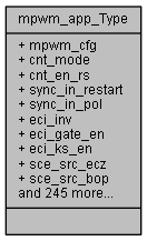
Data Fields | |
| union { | |
| __IOM uint32_t mpwm_cfg | |
| struct { | |
| __IOM uint32_t cnt_mode: 2 | |
| __IOM uint32_t cnt_en_rs: 1 | |
| __IOM uint32_t sync_in_restart: 1 | |
| __IOM uint32_t sync_in_pol: 1 | |
| __IOM uint32_t eci_inv: 1 | |
| __IOM uint32_t eci_gate_en: 1 | |
| __IOM uint32_t eci_ks_en: 1 | |
| __IOM uint32_t sce_src_ecz: 1 | |
| __IOM uint32_t sce_src_bop: 1 | |
| __IOM uint32_t sce_src_mop: 1 | |
| __IOM uint32_t evt_cnt_top: 5 | |
| __IOM uint32_t eci_fil_thresh: 8 | |
| __IOM uint32_t bf_align0: 8 | |
| } mpwm_cfg_b | |
| }; | |
| union { | |
| __IOM uint32_t mpwm_cnt_max | |
| struct { | |
| __IOM uint32_t val: 16 | |
| __IOM uint32_t bf_align0: 16 | |
| } mpwm_cnt_max_b | |
| }; | |
| union { | |
| __IOM uint32_t mpwm_cnt_ps_max | |
| struct { | |
| __IOM uint32_t val: 8 | |
| __IOM uint32_t bf_align0: 24 | |
| } mpwm_cnt_ps_max_b | |
| }; | |
| union { | |
| __IOM uint32_t mpwm_dt | |
| struct { | |
| __IOM uint32_t rise_val: 8 | |
| __IOM uint32_t fall_val: 8 | |
| __IOM uint32_t bf_align0: 16 | |
| } mpwm_dt_b | |
| }; | |
| union { | |
| __IOM uint32_t mpwm_ocfg | |
| struct { | |
| __IOM uint32_t osel0: 1 | |
| __IOM uint32_t osel1: 1 | |
| __IOM uint32_t osel2: 1 | |
| __IOM uint32_t osel3: 1 | |
| __IOM uint32_t osel4: 1 | |
| __IOM uint32_t osel5: 1 | |
| __IOM uint32_t bf_align0: 1 | |
| __IOM uint32_t oe0: 1 | |
| __IOM uint32_t oe1: 1 | |
| __IOM uint32_t oe2: 1 | |
| __IOM uint32_t oe3: 1 | |
| __IOM uint32_t oe4: 1 | |
| __IOM uint32_t oe5: 1 | |
| __IOM uint32_t oinv0: 1 | |
| __IOM uint32_t oinv1: 1 | |
| __IOM uint32_t oinv2: 1 | |
| __IOM uint32_t oinv3: 1 | |
| __IOM uint32_t oinv4: 1 | |
| __IOM uint32_t oinv5: 1 | |
| __IOM uint32_t oeden0: 1 | |
| __IOM uint32_t oeden1: 1 | |
| __IOM uint32_t oeden2: 1 | |
| __IOM uint32_t oeden3: 1 | |
| __IOM uint32_t oeden4: 1 | |
| __IOM uint32_t oeden5: 1 | |
| __IOM uint32_t oedpol0: 1 | |
| __IOM uint32_t oedpol1: 1 | |
| __IOM uint32_t oedpol2: 1 | |
| __IOM uint32_t oedpol3: 1 | |
| __IOM uint32_t oedpol4: 1 | |
| __IOM uint32_t oedpol5: 1 | |
| __IOM uint32_t bf_align1: 1 | |
| } mpwm_ocfg_b | |
| }; | |
| union { | |
| __IOM uint32_t mpwm_cnt_max_s | |
| struct { | |
| __IOM uint32_t val: 16 | |
| __IOM uint32_t bf_align0: 16 | |
| } mpwm_cnt_max_s_b | |
| }; | |
| union { | |
| __IOM uint32_t mpwm_dt_s | |
| struct { | |
| __IOM uint32_t rise_val: 8 | |
| __IOM uint32_t fall_val: 8 | |
| __IOM uint32_t bf_align0: 16 | |
| } mpwm_dt_s_b | |
| }; | |
| union { | |
| __IM uint32_t mpwm_status | |
| struct { | |
| __IM uint32_t running: 1 | |
| __IM uint32_t eci_val_unfil: 1 | |
| __IM uint32_t cnt_updown: 1 | |
| __IM uint32_t cnt_half: 1 | |
| __IM uint32_t bf_align0: 28 | |
| } mpwm_status_b | |
| }; | |
| union { | |
| __OM uint32_t mpwm_cmd | |
| struct { | |
| __OM uint32_t start: 1 | |
| __OM uint32_t stop: 1 | |
| __OM uint32_t restart: 1 | |
| __OM uint32_t sce_emit: 1 | |
| __OM uint32_t evt_cnt_rst: 1 | |
| __OM uint32_t eci_ks_rst: 1 | |
| __OM uint32_t bf_align0: 26 | |
| } mpwm_cmd_b | |
| }; | |
| union { | |
| __IM uint32_t mpwm_cnt | |
| struct { | |
| __IM uint32_t val: 16 | |
| __IM uint32_t bf_align0: 16 | |
| } mpwm_cnt_b | |
| }; | |
| union { | |
| __IM uint32_t mpwm_ecnt | |
| struct { | |
| __IM uint32_t val: 16 | |
| __IM uint32_t bf_align0: 16 | |
| } mpwm_ecnt_b | |
| }; | |
| union { | |
| __IM uint32_t mpwm_cnt_rs | |
| struct { | |
| __IM uint32_t cnt_val: 16 | |
| __IM uint32_t ps_val: 8 | |
| __IM uint32_t bf_align0: 8 | |
| } mpwm_cnt_rs_b | |
| }; | |
| union { | |
| __IM uint32_t mpwm_cnt_ps | |
| struct { | |
| __IM uint32_t val: 8 | |
| __IM uint32_t bf_align0: 24 | |
| } mpwm_cnt_ps_b | |
| }; | |
| union { | |
| __IM uint32_t mpwm_evt_cnt | |
| struct { | |
| __IM uint32_t val: 5 | |
| __IM uint32_t bf_align0: 27 | |
| } mpwm_evt_cnt_b | |
| }; | |
| union { | |
| __IOM uint32_t mpwm_bc_s | |
| struct { | |
| __IOM uint32_t val: 1 | |
| __IOM uint32_t bf_align0: 31 | |
| } mpwm_bc_s_b | |
| }; | |
| union { | |
| __IOM uint32_t mpwm_bc | |
| struct { | |
| __IOM uint32_t val: 1 | |
| __IOM uint32_t bf_align0: 31 | |
| } mpwm_bc_b | |
| }; | |
| __IM uint32_t | RESERVED [48] |
| union { | |
| __IOM uint32_t mpwm_ch0_cmp0_s | |
| struct { | |
| __IOM uint32_t val: 16 | |
| __IOM uint32_t bf_align0: 16 | |
| } mpwm_ch0_cmp0_s_b | |
| }; | |
| union { | |
| __IOM uint32_t mpwm_ch0_cmp1_s | |
| struct { | |
| __IOM uint32_t val: 16 | |
| __IOM uint32_t bf_align0: 16 | |
| } mpwm_ch0_cmp1_s_b | |
| }; | |
| union { | |
| __IOM uint32_t mpwm_ch0_cmp0 | |
| struct { | |
| __IOM uint32_t val: 16 | |
| __IOM uint32_t bf_align0: 16 | |
| } mpwm_ch0_cmp0_b | |
| }; | |
| union { | |
| __IOM uint32_t mpwm_ch0_cmp1 | |
| struct { | |
| __IOM uint32_t val: 16 | |
| __IOM uint32_t bf_align0: 16 | |
| } mpwm_ch0_cmp1_b | |
| }; | |
| union { | |
| __IOM uint32_t mpwm_ch0_muxin_s | |
| struct { | |
| __IOM uint32_t bl: 1 | |
| __IOM uint32_t bt: 1 | |
| __IOM uint32_t ab: 1 | |
| __IOM uint32_t bf_align0: 29 | |
| } mpwm_ch0_muxin_s_b | |
| }; | |
| union { | |
| __IOM uint32_t mpwm_ch0_muxin | |
| struct { | |
| __IOM uint32_t bl: 1 | |
| __IOM uint32_t bt: 1 | |
| __IOM uint32_t ab: 1 | |
| __IOM uint32_t bf_align0: 29 | |
| } mpwm_ch0_muxin_b | |
| }; | |
| __IM uint32_t | RESERVED1 [2] |
| union { | |
| __IOM uint32_t mpwm_ch1_cmp0_s | |
| struct { | |
| __IOM uint32_t val: 16 | |
| __IOM uint32_t bf_align0: 16 | |
| } mpwm_ch1_cmp0_s_b | |
| }; | |
| union { | |
| __IOM uint32_t mpwm_ch1_cmp1_s | |
| struct { | |
| __IOM uint32_t val: 16 | |
| __IOM uint32_t bf_align0: 16 | |
| } mpwm_ch1_cmp1_s_b | |
| }; | |
| union { | |
| __IOM uint32_t mpwm_ch1_cmp0 | |
| struct { | |
| __IOM uint32_t val: 16 | |
| __IOM uint32_t bf_align0: 16 | |
| } mpwm_ch1_cmp0_b | |
| }; | |
| union { | |
| __IOM uint32_t mpwm_ch1_cmp1 | |
| struct { | |
| __IOM uint32_t val: 16 | |
| __IOM uint32_t bf_align0: 16 | |
| } mpwm_ch1_cmp1_b | |
| }; | |
| union { | |
| __IOM uint32_t mpwm_ch1_muxin_s | |
| struct { | |
| __IOM uint32_t bl: 1 | |
| __IOM uint32_t bt: 1 | |
| __IOM uint32_t ab: 1 | |
| __IOM uint32_t bf_align0: 29 | |
| } mpwm_ch1_muxin_s_b | |
| }; | |
| union { | |
| __IOM uint32_t mpwm_ch1_muxin | |
| struct { | |
| __IOM uint32_t bl: 1 | |
| __IOM uint32_t bt: 1 | |
| __IOM uint32_t ab: 1 | |
| __IOM uint32_t bf_align0: 29 | |
| } mpwm_ch1_muxin_b | |
| }; | |
| __IM uint32_t | RESERVED2 [2] |
| union { | |
| __IOM uint32_t mpwm_ch2_cmp0_s | |
| struct { | |
| __IOM uint32_t val: 16 | |
| __IOM uint32_t bf_align0: 16 | |
| } mpwm_ch2_cmp0_s_b | |
| }; | |
| union { | |
| __IOM uint32_t mpwm_ch2_cmp1_s | |
| struct { | |
| __IOM uint32_t val: 16 | |
| __IOM uint32_t bf_align0: 16 | |
| } mpwm_ch2_cmp1_s_b | |
| }; | |
| union { | |
| __IOM uint32_t mpwm_ch2_cmp0 | |
| struct { | |
| __IOM uint32_t val: 16 | |
| __IOM uint32_t bf_align0: 16 | |
| } mpwm_ch2_cmp0_b | |
| }; | |
| union { | |
| __IOM uint32_t mpwm_ch2_cmp1 | |
| struct { | |
| __IOM uint32_t val: 16 | |
| __IOM uint32_t bf_align0: 16 | |
| } mpwm_ch2_cmp1_b | |
| }; | |
| union { | |
| __IOM uint32_t mpwm_ch2_muxin_s | |
| struct { | |
| __IOM uint32_t bl: 1 | |
| __IOM uint32_t bt: 1 | |
| __IOM uint32_t ab: 1 | |
| __IOM uint32_t bf_align0: 29 | |
| } mpwm_ch2_muxin_s_b | |
| }; | |
| union { | |
| __IOM uint32_t mpwm_ch2_muxin | |
| struct { | |
| __IOM uint32_t bl: 1 | |
| __IOM uint32_t bt: 1 | |
| __IOM uint32_t ab: 1 | |
| __IOM uint32_t bf_align0: 29 | |
| } mpwm_ch2_muxin_b | |
| }; | |
| __IM uint32_t | RESERVED3 [2] |
| union { | |
| __IOM uint32_t mpwm_ch3_cmp0_s | |
| struct { | |
| __IOM uint32_t val: 16 | |
| __IOM uint32_t bf_align0: 16 | |
| } mpwm_ch3_cmp0_s_b | |
| }; | |
| union { | |
| __IOM uint32_t mpwm_ch3_cmp1_s | |
| struct { | |
| __IOM uint32_t val: 16 | |
| __IOM uint32_t bf_align0: 16 | |
| } mpwm_ch3_cmp1_s_b | |
| }; | |
| union { | |
| __IOM uint32_t mpwm_ch3_cmp0 | |
| struct { | |
| __IOM uint32_t val: 16 | |
| __IOM uint32_t bf_align0: 16 | |
| } mpwm_ch3_cmp0_b | |
| }; | |
| union { | |
| __IOM uint32_t mpwm_ch3_cmp1 | |
| struct { | |
| __IOM uint32_t val: 16 | |
| __IOM uint32_t bf_align0: 16 | |
| } mpwm_ch3_cmp1_b | |
| }; | |
| union { | |
| __IOM uint32_t mpwm_ch3_muxin_s | |
| struct { | |
| __IOM uint32_t bl: 1 | |
| __IOM uint32_t bt: 1 | |
| __IOM uint32_t ab: 1 | |
| __IOM uint32_t bf_align0: 29 | |
| } mpwm_ch3_muxin_s_b | |
| }; | |
| union { | |
| __IOM uint32_t mpwm_ch3_muxin | |
| struct { | |
| __IOM uint32_t bl: 1 | |
| __IOM uint32_t bt: 1 | |
| __IOM uint32_t ab: 1 | |
| __IOM uint32_t bf_align0: 29 | |
| } mpwm_ch3_muxin_b | |
| }; | |
| __IM uint32_t | RESERVED4 [2] |
| union { | |
| __IOM uint32_t mpwm_ch4_cmp0_s | |
| struct { | |
| __IOM uint32_t val: 16 | |
| __IOM uint32_t bf_align0: 16 | |
| } mpwm_ch4_cmp0_s_b | |
| }; | |
| union { | |
| __IOM uint32_t mpwm_ch4_cmp1_s | |
| struct { | |
| __IOM uint32_t val: 16 | |
| __IOM uint32_t bf_align0: 16 | |
| } mpwm_ch4_cmp1_s_b | |
| }; | |
| union { | |
| __IOM uint32_t mpwm_ch4_cmp0 | |
| struct { | |
| __IOM uint32_t val: 16 | |
| __IOM uint32_t bf_align0: 16 | |
| } mpwm_ch4_cmp0_b | |
| }; | |
| union { | |
| __IOM uint32_t mpwm_ch4_cmp1 | |
| struct { | |
| __IOM uint32_t val: 16 | |
| __IOM uint32_t bf_align0: 16 | |
| } mpwm_ch4_cmp1_b | |
| }; | |
| union { | |
| __IOM uint32_t mpwm_ch4_muxin_s | |
| struct { | |
| __IOM uint32_t bl: 1 | |
| __IOM uint32_t bt: 1 | |
| __IOM uint32_t ab: 1 | |
| __IOM uint32_t bf_align0: 29 | |
| } mpwm_ch4_muxin_s_b | |
| }; | |
| union { | |
| __IOM uint32_t mpwm_ch4_muxin | |
| struct { | |
| __IOM uint32_t bl: 1 | |
| __IOM uint32_t bt: 1 | |
| __IOM uint32_t ab: 1 | |
| __IOM uint32_t bf_align0: 29 | |
| } mpwm_ch4_muxin_b | |
| }; | |
| __IM uint32_t | RESERVED5 [2] |
| union { | |
| __IOM uint32_t mpwm_ch5_cmp0_s | |
| struct { | |
| __IOM uint32_t val: 16 | |
| __IOM uint32_t bf_align0: 16 | |
| } mpwm_ch5_cmp0_s_b | |
| }; | |
| union { | |
| __IOM uint32_t mpwm_ch5_cmp1_s | |
| struct { | |
| __IOM uint32_t val: 16 | |
| __IOM uint32_t bf_align0: 16 | |
| } mpwm_ch5_cmp1_s_b | |
| }; | |
| union { | |
| __IOM uint32_t mpwm_ch5_cmp0 | |
| struct { | |
| __IOM uint32_t val: 16 | |
| __IOM uint32_t bf_align0: 16 | |
| } mpwm_ch5_cmp0_b | |
| }; | |
| union { | |
| __IOM uint32_t mpwm_ch5_cmp1 | |
| struct { | |
| __IOM uint32_t val: 16 | |
| __IOM uint32_t bf_align0: 16 | |
| } mpwm_ch5_cmp1_b | |
| }; | |
| union { | |
| __IOM uint32_t mpwm_ch5_muxin_s | |
| struct { | |
| __IOM uint32_t bl: 1 | |
| __IOM uint32_t bt: 1 | |
| __IOM uint32_t ab: 1 | |
| __IOM uint32_t bf_align0: 29 | |
| } mpwm_ch5_muxin_s_b | |
| }; | |
| union { | |
| __IOM uint32_t mpwm_ch5_muxin | |
| struct { | |
| __IOM uint32_t bl: 1 | |
| __IOM uint32_t bt: 1 | |
| __IOM uint32_t ab: 1 | |
| __IOM uint32_t bf_align0: 29 | |
| } mpwm_ch5_muxin_b | |
| }; | |
| __IM uint32_t | RESERVED6 [2] |
| union { | |
| __IOM uint32_t mpwm_irq_raw | |
| struct { | |
| __IOM uint32_t ecz: 1 | |
| __IOM uint32_t bop: 1 | |
| __IOM uint32_t mop: 1 | |
| __IOM uint32_t eci_val: 1 | |
| __IOM uint32_t eci_ks_state: 1 | |
| __IOM uint32_t oede: 6 | |
| __IOM uint32_t bf_align0: 21 | |
| } mpwm_irq_raw_b | |
| }; | |
| union { | |
| __IM uint32_t mpwm_irq_masked | |
| struct { | |
| __IM uint32_t ecz: 1 | |
| __IM uint32_t bop: 1 | |
| __IM uint32_t mop: 1 | |
| __IM uint32_t eci_val: 1 | |
| __IM uint32_t eci_ks_state: 1 | |
| __IM uint32_t oede: 6 | |
| __IM uint32_t bf_align0: 21 | |
| } mpwm_irq_masked_b | |
| }; | |
| union { | |
| __IOM uint32_t mpwm_irq_msk_set | |
| struct { | |
| __IOM uint32_t ecz: 1 | |
| __IOM uint32_t bop: 1 | |
| __IOM uint32_t mop: 1 | |
| __IOM uint32_t eci_val: 1 | |
| __IOM uint32_t eci_ks_state: 1 | |
| __IOM uint32_t oede: 6 | |
| __IOM uint32_t bf_align0: 21 | |
| } mpwm_irq_msk_set_b | |
| }; | |
| union { | |
| __IOM uint32_t mpwm_irq_msk_reset | |
| struct { | |
| __IOM uint32_t ecz: 1 | |
| __IOM uint32_t bop: 1 | |
| __IOM uint32_t mop: 1 | |
| __IOM uint32_t eci_val: 1 | |
| __IOM uint32_t eci_ks_state: 1 | |
| __IOM uint32_t oede: 6 | |
| __IOM uint32_t bf_align0: 21 | |
| } mpwm_irq_msk_reset_b | |
| }; | |
| union { | |
| __IM uint32_t mpwm_irq_no | |
| struct { | |
| __IM uint32_t val: 4 | |
| __IM uint32_t bf_align0: 28 | |
| } mpwm_irq_no_b | |
| }; | |
mpwm_app (mpwm_app)
Definition at line 29462 of file netx90_app.h.
| union { ... } |
< (@ 0xFF802400) mpwm_app Structure
| union { ... } |
| union { ... } |
| union { ... } |
| union { ... } |
| union { ... } |
| union { ... } |
| union { ... } |
| union { ... } |
| union { ... } |
| union { ... } |
| union { ... } |
| union { ... } |
| union { ... } |
| union { ... } |
| union { ... } |
| union { ... } |
| union { ... } |
| union { ... } |
| union { ... } |
| union { ... } |
| union { ... } |
| union { ... } |
| union { ... } |
| union { ... } |
| union { ... } |
| union { ... } |
| union { ... } |
| union { ... } |
| union { ... } |
| union { ... } |
| union { ... } |
| union { ... } |
| union { ... } |
| union { ... } |
| union { ... } |
| union { ... } |
| union { ... } |
| union { ... } |
| union { ... } |
| union { ... } |
| union { ... } |
| union { ... } |
| union { ... } |
| union { ... } |
| union { ... } |
| union { ... } |
| union { ... } |
| union { ... } |
| union { ... } |
| union { ... } |
| union { ... } |
| union { ... } |
| union { ... } |
| union { ... } |
| union { ... } |
| union { ... } |
| __IOM uint32_t mpwm_app_Type::ab |
[2..2] above
Definition at line 29818 of file netx90_app.h.
| __IOM uint32_t mpwm_app_Type::bf_align0 |
[31..24] bitField alignment value for aeabi compatibility
[31..16] bitField alignment value for aeabi compatibility
[31..8] bitField alignment value for aeabi compatibility
[6..6] bitField alignment value for aeabi compatibility
[31..1] bitField alignment value for aeabi compatibility
[31..3] bitField alignment value for aeabi compatibility
[31..11] bitField alignment value for aeabi compatibility
Definition at line 29508 of file netx90_app.h.
| __IM uint32_t mpwm_app_Type::bf_align0 |
[31..4] bitField alignment value for aeabi compatibility
[31..16] bitField alignment value for aeabi compatibility
[31..24] bitField alignment value for aeabi compatibility
[31..8] bitField alignment value for aeabi compatibility
[31..5] bitField alignment value for aeabi compatibility
[31..11] bitField alignment value for aeabi compatibility
Definition at line 29651 of file netx90_app.h.
| __OM uint32_t mpwm_app_Type::bf_align0 |
[31..6] bitField alignment value for aeabi compatibility
Definition at line 29676 of file netx90_app.h.
| __IOM uint32_t mpwm_app_Type::bf_align1 |
[31..31] bitField alignment value for aeabi compatibility
Definition at line 29604 of file netx90_app.h.
| __IOM uint32_t mpwm_app_Type::bl |
[0..0] below
Definition at line 29816 of file netx90_app.h.
| __IOM uint32_t mpwm_app_Type::bop |
[1..1] event: beginning of PWM period bit
Definition at line 30237 of file netx90_app.h.
| __IM uint32_t mpwm_app_Type::bop |
[1..1] event: beginning of PWM period bit
Definition at line 30253 of file netx90_app.h.
| __IOM uint32_t mpwm_app_Type::bt |
[1..1] between
Definition at line 29817 of file netx90_app.h.
| __IOM uint32_t mpwm_app_Type::cnt_en_rs |
[2..2] cnt_en_rs When this bit is one and sync_in is active, save the value of MPWM_CNT to the MPWM_CNT_RS (rs = read sync) register.
Definition at line 29471 of file netx90_app.h.
| __IM uint32_t mpwm_app_Type::cnt_half |
[3..3] count half: 0: counter is in first half period of triangle mode or inverted triangle mode or counter is in sawtooth or inverse sawtooth mode. 1: counter is in second half period of triangle mode or inverted triangle mode
Definition at line 29647 of file netx90_app.h.
| __IOM uint32_t mpwm_app_Type::cnt_mode |
[1..0] Counter mode: 00: sawtooth 01: triangle 10: inv sawtooth 11: inv triangle
Definition at line 29469 of file netx90_app.h.
| __IM uint32_t mpwm_app_Type::cnt_updown |
[2..2] count updown 0: counter is counting down 1: counter is counting up
Definition at line 29645 of file netx90_app.h.
| __IM uint32_t mpwm_app_Type::cnt_val |
[15..0] saved value of the MPWM_CNT register
Definition at line 29714 of file netx90_app.h.
| __IOM uint32_t mpwm_app_Type::eci_fil_thresh |
[23..16] ECI filter threshold: Threshold value for the error condition input integral filter.
Definition at line 29506 of file netx90_app.h.
| __IOM uint32_t mpwm_app_Type::eci_gate_en |
[6..6] eci_gate_en Set 1 to gate all pwm outputs with the integral filtered error control input. This means that the outputs will be disabled asynchronously whenever eci is active.
Definition at line 29482 of file netx90_app.h.
| __IOM uint32_t mpwm_app_Type::eci_inv |
[5..5] eci_inv This bit controls the polarity of the error condition input (eci). Set 0 for active high eci, 1 for active low eci.
Definition at line 29479 of file netx90_app.h.
| __IOM uint32_t mpwm_app_Type::eci_ks_en |
[7..7] eci_ks_en Set 1 to enable synchronous error condition input (eci) kill switch. The synchronous eci kill switch is a flip flop that is set once eci is active. The eci kill switch can only be reset through MPWM_ECI_CMD. When the eci kill switch is set, all PWM module outputs are disabled.
Definition at line 29485 of file netx90_app.h.
| __OM uint32_t mpwm_app_Type::eci_ks_rst |
[5..5] ECI kill switch reset: Command register to reset the eci kill switch.
Definition at line 29674 of file netx90_app.h.
| __IOM uint32_t mpwm_app_Type::eci_ks_state |
[4..4] status: error condition kill switch state bit
Definition at line 30241 of file netx90_app.h.
| __IM uint32_t mpwm_app_Type::eci_ks_state |
[4..4] status: error condition kill switch state bit
Definition at line 30257 of file netx90_app.h.
| __IOM uint32_t mpwm_app_Type::eci_val |
[3..3] status: eci_val error condition input value bit after filter
Definition at line 30239 of file netx90_app.h.
| __IM uint32_t mpwm_app_Type::eci_val |
[3..3] status: eci_val error condition input value bit after filter
Definition at line 30255 of file netx90_app.h.
| __IM uint32_t mpwm_app_Type::eci_val_unfil |
[1..1] Error Condition Input unfiltered: Read the current value of the error condition input before the digital integral filter. This bit is corrected for polarity, which means it reads zero for inactive, one for active.
Definition at line 29641 of file netx90_app.h.
| __IOM uint32_t mpwm_app_Type::ecz |
[0..0] event: evt_counter reached zero bit
Definition at line 30236 of file netx90_app.h.
| __IM uint32_t mpwm_app_Type::ecz |
[0..0] event: evt_counter reached zero bit
Definition at line 30252 of file netx90_app.h.
| __OM uint32_t mpwm_app_Type::evt_cnt_rst |
[4..4] Event Counter Reset
Definition at line 29673 of file netx90_app.h.
| __IOM uint32_t mpwm_app_Type::evt_cnt_top |
[15..11] evt_cnt_top Used to specify the maximum value of EVT_CNT. When EVT_CNT is zero and a begin of period )BOP) event occurs, an event counter zero (ECZ) event is emitted and EVT_CNT is reset to evt_cnt_top. If an begin of period event occurs and EVT_CNT is not zero, EVT_CNT is decremented. This mechanism can be used as an event prescaler to reduce the number of period interrupts from the MPWM module. Examples: If evt_cnt_top is zero, ECZ events and BOP events will coincide. If evt_cnt_top is one, ECZ events wi
Definition at line 29497 of file netx90_app.h.
| __IOM uint32_t mpwm_app_Type::fall_val |
[15..8] Dead time cycles at falling edge of PWM signal
[15..8] Dead time shadow value for falling edge of PWM signal
Definition at line 29556 of file netx90_app.h.
| __IOM uint32_t mpwm_app_Type::mop |
[2..2] event: middle of PWM period bit
Definition at line 30238 of file netx90_app.h.
| __IM uint32_t mpwm_app_Type::mop |
[2..2] event: middle of PWM period bit
Definition at line 30254 of file netx90_app.h.
| __IOM uint32_t mpwm_app_Type::mpwm_bc |
(@ 0x0000003C) Brake chopper register: The brake chopper output signal is determined by the value of this register.
Definition at line 29759 of file netx90_app.h.
| struct { ... } mpwm_app_Type::mpwm_bc_b |
| __IOM uint32_t mpwm_app_Type::mpwm_bc_s |
(@ 0x00000038) Brake chopper shadow register: Shadow register for the brake chopper output
Definition at line 29749 of file netx90_app.h.
| struct { ... } mpwm_app_Type::mpwm_bc_s_b |
| __IOM uint32_t mpwm_app_Type::mpwm_cfg |
(@ 0x00000000) Config register: General config bits for the MPWM module.
Definition at line 29465 of file netx90_app.h.
| struct { ... } mpwm_app_Type::mpwm_cfg_b |
| __IOM uint32_t mpwm_app_Type::mpwm_ch0_cmp0 |
(@ 0x00000108) Channel 0 compare value 0 register: Compare value 0 for channel 0.
Definition at line 29791 of file netx90_app.h.
| struct { ... } mpwm_app_Type::mpwm_ch0_cmp0_b |
| __IOM uint32_t mpwm_app_Type::mpwm_ch0_cmp0_s |
(@ 0x00000100) Channel 0 compare value 0 shadow register: Compare value 0 shadow register for channel 0.
Definition at line 29771 of file netx90_app.h.
| struct { ... } mpwm_app_Type::mpwm_ch0_cmp0_s_b |
| __IOM uint32_t mpwm_app_Type::mpwm_ch0_cmp1 |
(@ 0x0000010C) Channel 0 compare value 1 register: Compare value 1 for channel 0.
Definition at line 29801 of file netx90_app.h.
| struct { ... } mpwm_app_Type::mpwm_ch0_cmp1_b |
| __IOM uint32_t mpwm_app_Type::mpwm_ch0_cmp1_s |
(@ 0x00000104) Channel 0 compare value 1 shadow register: Compare value 1 shadow register for channel 0.
Definition at line 29781 of file netx90_app.h.
| struct { ... } mpwm_app_Type::mpwm_ch0_cmp1_s_b |
| __IOM uint32_t mpwm_app_Type::mpwm_ch0_muxin |
(@ 0x00000114) Channel 0 multiplexer input register: This register is central in determining the direct PWM output value of channel 0. When (CNT < CHX_CMP0) and (CNT < CHX_CMP1), then the direct PWM output signal is equal to CHX_MUXIN.bl (counter value is BeLow both compare values). When (CNT >= CHX_CMP0) and (CNT >= CHX_CMP1), then the direct PWM output signal is equal to CHX_MUXIN.ab (counter value is ABove both compare values). If neither is the case, CNT is BeTween CHX_CMP0 and CHX_CMP1 and
Definition at line 29824 of file netx90_app.h.
| struct { ... } mpwm_app_Type::mpwm_ch0_muxin_b |
| __IOM uint32_t mpwm_app_Type::mpwm_ch0_muxin_s |
(@ 0x00000110) Channel 0 multiplexer input shadow register: Shadow register for channel 0 multiplexer input register.
Definition at line 29811 of file netx90_app.h.
| struct { ... } mpwm_app_Type::mpwm_ch0_muxin_s_b |
| __IOM uint32_t mpwm_app_Type::mpwm_ch1_cmp0 |
(@ 0x00000128) Channel 1 compare value 0 register: Compare value 0 for channel 1.
Definition at line 29867 of file netx90_app.h.
| struct { ... } mpwm_app_Type::mpwm_ch1_cmp0_b |
| __IOM uint32_t mpwm_app_Type::mpwm_ch1_cmp0_s |
(@ 0x00000120) Channel 1 compare value 0 shadow register: Compare value 0 shadow register for channel 1.
Definition at line 29847 of file netx90_app.h.
| struct { ... } mpwm_app_Type::mpwm_ch1_cmp0_s_b |
| __IOM uint32_t mpwm_app_Type::mpwm_ch1_cmp1 |
(@ 0x0000012C) Channel 1 compare value 1 register: Compare value 1 for channel 1.
Definition at line 29877 of file netx90_app.h.
| struct { ... } mpwm_app_Type::mpwm_ch1_cmp1_b |
| __IOM uint32_t mpwm_app_Type::mpwm_ch1_cmp1_s |
(@ 0x00000124) Channel 1 compare value 1 shadow register: Compare value 1 shadow register for channel 1.
Definition at line 29857 of file netx90_app.h.
| struct { ... } mpwm_app_Type::mpwm_ch1_cmp1_s_b |
| __IOM uint32_t mpwm_app_Type::mpwm_ch1_muxin |
(@ 0x00000134) Channel 1 multiplexer input register: This register is central in determining the direct PWM output value of channel 1. When (CHX_CMP0 $>=$ CNT) and (CHX_CMP1 $>=$ CNT), the direct PWM output signal is equal to CHX_MUXIN.bl (counter value is below both compare values). When (CHX_CMP0 $>=$ CNT) xor (CHX_CMP1 $>=$ CNT) is true, then the direct PWM output signal is equal to CHX_MUXIN.bt (counter value is between both compare values). When not (CHX_CMP0 $>=$ CNT) and not (CHX_CMP1 $>=$
Definition at line 29900 of file netx90_app.h.
| struct { ... } mpwm_app_Type::mpwm_ch1_muxin_b |
| __IOM uint32_t mpwm_app_Type::mpwm_ch1_muxin_s |
(@ 0x00000130) Channel 1 multiplexer input shadow register: Shadow register for channel 1 multiplexer input register.
Definition at line 29887 of file netx90_app.h.
| struct { ... } mpwm_app_Type::mpwm_ch1_muxin_s_b |
| __IOM uint32_t mpwm_app_Type::mpwm_ch2_cmp0 |
(@ 0x00000148) Channel 2 compare value 0 register: Compare value 0 for channel 2.
Definition at line 29943 of file netx90_app.h.
| struct { ... } mpwm_app_Type::mpwm_ch2_cmp0_b |
| __IOM uint32_t mpwm_app_Type::mpwm_ch2_cmp0_s |
(@ 0x00000140) Channel 2 compare value 0 shadow register: Compare value 0 shadow register for channel 2.
Definition at line 29923 of file netx90_app.h.
| struct { ... } mpwm_app_Type::mpwm_ch2_cmp0_s_b |
| __IOM uint32_t mpwm_app_Type::mpwm_ch2_cmp1 |
(@ 0x0000014C) Channel 2 compare value 1 register: Compare value 1 for channel 2.
Definition at line 29953 of file netx90_app.h.
| struct { ... } mpwm_app_Type::mpwm_ch2_cmp1_b |
| __IOM uint32_t mpwm_app_Type::mpwm_ch2_cmp1_s |
(@ 0x00000144) Channel 2 compare value 1 shadow register: Compare value 1 shadow register for channel 2.
Definition at line 29933 of file netx90_app.h.
| struct { ... } mpwm_app_Type::mpwm_ch2_cmp1_s_b |
| __IOM uint32_t mpwm_app_Type::mpwm_ch2_muxin |
(@ 0x00000154) Channel 2 multiplexer input register: This register is central in determining the direct PWM output value of channel 2. When (CHX_CMP0 $>=$ CNT) and (CHX_CMP1 $>=$ CNT), the direct PWM output signal is equal to CHX_MUXIN.bl (counter value is below both compare values). When (CHX_CMP0 $>=$ CNT) xor (CHX_CMP1 $>=$ CNT) is true, then the direct PWM output signal is equal to CHX_MUXIN.bt (counter value is between both compare values). When not (CHX_CMP0 $>=$ CNT) and not (CHX_CMP1 $>=$
Definition at line 29976 of file netx90_app.h.
| struct { ... } mpwm_app_Type::mpwm_ch2_muxin_b |
| __IOM uint32_t mpwm_app_Type::mpwm_ch2_muxin_s |
(@ 0x00000150) Channel 2 multiplexer input shadow register: Shadow register for channel 2 multiplexer input register.
Definition at line 29963 of file netx90_app.h.
| struct { ... } mpwm_app_Type::mpwm_ch2_muxin_s_b |
| __IOM uint32_t mpwm_app_Type::mpwm_ch3_cmp0 |
(@ 0x00000168) Channel 3 compare value 0 register: Compare value 0 for channel 3.
Definition at line 30019 of file netx90_app.h.
| struct { ... } mpwm_app_Type::mpwm_ch3_cmp0_b |
| __IOM uint32_t mpwm_app_Type::mpwm_ch3_cmp0_s |
(@ 0x00000160) Channel 3 compare value 0 shadow register: Compare value 0 shadow register for channel 3.
Definition at line 29999 of file netx90_app.h.
| struct { ... } mpwm_app_Type::mpwm_ch3_cmp0_s_b |
| __IOM uint32_t mpwm_app_Type::mpwm_ch3_cmp1 |
(@ 0x0000016C) Channel 3 compare value 1 register: Compare value 1 for channel 3.
Definition at line 30029 of file netx90_app.h.
| struct { ... } mpwm_app_Type::mpwm_ch3_cmp1_b |
| __IOM uint32_t mpwm_app_Type::mpwm_ch3_cmp1_s |
(@ 0x00000164) Channel 3 compare value 1 shadow register: Compare value 1 shadow register for channel 3.
Definition at line 30009 of file netx90_app.h.
| struct { ... } mpwm_app_Type::mpwm_ch3_cmp1_s_b |
| __IOM uint32_t mpwm_app_Type::mpwm_ch3_muxin |
(@ 0x00000174) Channel 3 multiplexer input register: This register is central in determining the direct PWM output value of channel 3. When (CHX_CMP0 $>=$ CNT) and (CHX_CMP1 $>=$ CNT), the direct PWM output signal is equal to CHX_MUXIN.bl (counter value is below both compare values). When (CHX_CMP0 $>=$ CNT) xor (CHX_CMP1 $>=$ CNT) is true, then the direct PWM output signal is equal to CHX_MUXIN.bt (counter value is between both compare values). When not (CHX_CMP0 $>=$ CNT) and not (CHX_CMP1 $>=$
Definition at line 30052 of file netx90_app.h.
| struct { ... } mpwm_app_Type::mpwm_ch3_muxin_b |
| __IOM uint32_t mpwm_app_Type::mpwm_ch3_muxin_s |
(@ 0x00000170) Channel 3 multiplexer input shadow register: Shadow register for channel 3 multiplexer input register.
Definition at line 30039 of file netx90_app.h.
| struct { ... } mpwm_app_Type::mpwm_ch3_muxin_s_b |
| __IOM uint32_t mpwm_app_Type::mpwm_ch4_cmp0 |
(@ 0x00000188) Channel 4 compare value 0 register: Compare value 0 for channel 4.
Definition at line 30095 of file netx90_app.h.
| struct { ... } mpwm_app_Type::mpwm_ch4_cmp0_b |
| __IOM uint32_t mpwm_app_Type::mpwm_ch4_cmp0_s |
(@ 0x00000180) Channel 4 compare value 0 shadow register: Compare value 0 shadow register for channel 4.
Definition at line 30075 of file netx90_app.h.
| struct { ... } mpwm_app_Type::mpwm_ch4_cmp0_s_b |
| __IOM uint32_t mpwm_app_Type::mpwm_ch4_cmp1 |
(@ 0x0000018C) Channel 4 compare value 1 register: Compare value 1 for channel 4.
Definition at line 30105 of file netx90_app.h.
| struct { ... } mpwm_app_Type::mpwm_ch4_cmp1_b |
| __IOM uint32_t mpwm_app_Type::mpwm_ch4_cmp1_s |
(@ 0x00000184) Channel 4 compare value 1 shadow register: Compare value 1 shadow register for channel 4.
Definition at line 30085 of file netx90_app.h.
| struct { ... } mpwm_app_Type::mpwm_ch4_cmp1_s_b |
| __IOM uint32_t mpwm_app_Type::mpwm_ch4_muxin |
(@ 0x00000194) Channel 4 multiplexer input register: This register is central in determining the direct PWM output value of channel 4. When (CHX_CMP0 $>=$ CNT) and (CHX_CMP1 $>=$ CNT), the direct PWM output signal is equal to CHX_MUXIN.bl (counter value is below both compare values). When (CHX_CMP0 $>=$ CNT) xor (CHX_CMP1 $>=$ CNT) is true, then the direct PWM output signal is equal to CHX_MUXIN.bt (counter value is between both compare values). When not (CHX_CMP0 $>=$ CNT) and not (CHX_CMP1 $>=$
Definition at line 30128 of file netx90_app.h.
| struct { ... } mpwm_app_Type::mpwm_ch4_muxin_b |
| __IOM uint32_t mpwm_app_Type::mpwm_ch4_muxin_s |
(@ 0x00000190) Channel 4 multiplexer input shadow register: Shadow register for channel 4 multiplexer input register.
Definition at line 30115 of file netx90_app.h.
| struct { ... } mpwm_app_Type::mpwm_ch4_muxin_s_b |
| __IOM uint32_t mpwm_app_Type::mpwm_ch5_cmp0 |
(@ 0x000001A8) Channel 5 compare value 0 register: Compare value 0 for channel 5.
Definition at line 30171 of file netx90_app.h.
| struct { ... } mpwm_app_Type::mpwm_ch5_cmp0_b |
| __IOM uint32_t mpwm_app_Type::mpwm_ch5_cmp0_s |
(@ 0x000001A0) Channel 5 compare value 0 shadow register: Compare value 0 shadow register for channel 5.
Definition at line 30151 of file netx90_app.h.
| struct { ... } mpwm_app_Type::mpwm_ch5_cmp0_s_b |
| __IOM uint32_t mpwm_app_Type::mpwm_ch5_cmp1 |
(@ 0x000001AC) Channel 5 compare value 1 register: Compare value 1 for channel 5.
Definition at line 30181 of file netx90_app.h.
| struct { ... } mpwm_app_Type::mpwm_ch5_cmp1_b |
| __IOM uint32_t mpwm_app_Type::mpwm_ch5_cmp1_s |
(@ 0x000001A4) Channel 5 compare value 1 shadow register: Compare value 1 shadow register for channel 5.
Definition at line 30161 of file netx90_app.h.
| struct { ... } mpwm_app_Type::mpwm_ch5_cmp1_s_b |
| __IOM uint32_t mpwm_app_Type::mpwm_ch5_muxin |
(@ 0x000001B4) Channel 5 multiplexer input register: This register is central in determining the direct PWM output value of channel 5. When (CHX_CMP0 $>=$ CNT) and (CHX_CMP1 $>=$ CNT), the direct PWM output signal is equal to CHX_MUXIN.bl (counter value is below both compare values). When (CHX_CMP0 $>=$ CNT) xor (CHX_CMP1 $>=$ CNT) is true, then the direct PWM output signal is equal to CHX_MUXIN.bt (counter value is between both compare values). When not (CHX_CMP0 $>=$ CNT) and not (CHX_CMP1 $>=$
Definition at line 30204 of file netx90_app.h.
| struct { ... } mpwm_app_Type::mpwm_ch5_muxin_b |
| __IOM uint32_t mpwm_app_Type::mpwm_ch5_muxin_s |
(@ 0x000001B0) Channel 5 multiplexer input shadow register: Shadow register for channel 5 multiplexer input register.
Definition at line 30191 of file netx90_app.h.
| struct { ... } mpwm_app_Type::mpwm_ch5_muxin_s_b |
| __OM uint32_t mpwm_app_Type::mpwm_cmd |
(@ 0x00000020) Command register:
Definition at line 29656 of file netx90_app.h.
| struct { ... } mpwm_app_Type::mpwm_cmd_b |
| __IM uint32_t mpwm_app_Type::mpwm_cnt |
(@ 0x00000024) Counter: Global counter. Used for all the comparisons that then generate the PWM signals. See counter behaviour diagram.
Definition at line 29681 of file netx90_app.h.
| struct { ... } mpwm_app_Type::mpwm_cnt_b |
| __IOM uint32_t mpwm_app_Type::mpwm_cnt_max |
(@ 0x00000004) Counter top register: This is the maximum / top value for the PWM counter. In inverse sawtooth mode, MPWM_CNT will be loaded with MPWM_CNT_MAX after reaching zero or when restarting the counter. In sawtooth mode, MPWM_CNT will be reset to zero after reaching MPWM_CNT_MAX. In inverse sawtooth mode, MPWM_CNT will be set to MPWM_CNT_MAX when restarting the counter, and when it reaches MPWM_CNT_MAX while counting up, it will change to counting down. In inverse sawtooth mode, when MPWM_
Definition at line 29513 of file netx90_app.h.
| struct { ... } mpwm_app_Type::mpwm_cnt_max_b |
| __IOM uint32_t mpwm_app_Type::mpwm_cnt_max_s |
(@ 0x00000014) Counter top shadow register: Shadow register for MPWM_CNT_TOP. After writing this register, an internal flag is set. If the internal flag is set, at the next occurence of a shadow copy event cnt_top will be overwritten by MPWM_CNT_MAX_S and the internal flag will be reset.
Definition at line 29609 of file netx90_app.h.
| struct { ... } mpwm_app_Type::mpwm_cnt_max_s_b |
| __IM uint32_t mpwm_app_Type::mpwm_cnt_ps |
(@ 0x00000030) Counter prescaler register: Internal counter that is responsible for determining, in which clock cycles cnt will be incremented / decremented. MPWM_CNT_PS is reloaded with MPWM_CNT_PS_MAX when it reaches zero. In every clock cycle, in which MPWM_CNT_PS is zero, cnt will be incremented / decremented.
Definition at line 29721 of file netx90_app.h.
| struct { ... } mpwm_app_Type::mpwm_cnt_ps_b |
| __IOM uint32_t mpwm_app_Type::mpwm_cnt_ps_max |
(@ 0x00000008) Counter prescaler max value register: The values of this register determines how often MPWM_CNT and the counters in the dead time generators will be updated. When setting MPWM_CNT_PS_MAX to n, MPWM_CNT will be updated every n + 1 system clock cycles. This register can be used to slow down operation of the counter.
Definition at line 29532 of file netx90_app.h.
| struct { ... } mpwm_app_Type::mpwm_cnt_ps_max_b |
| __IM uint32_t mpwm_app_Type::mpwm_cnt_rs |
(@ 0x0000002C) Counter save register: When CFG.cnt_en_rs (rs = read sync) is set, this register is used to save the value of the MPWM_CNT and MPWM_CNT_PS register every time that sync_in becomes active.
Definition at line 29707 of file netx90_app.h.
| struct { ... } mpwm_app_Type::mpwm_cnt_rs_b |
| __IOM uint32_t mpwm_app_Type::mpwm_dt |
(@ 0x0000000C) Dead time register: This is the number of dead (LS and HS off) cycles (prescaled by MPWM_CNT_PS) that the dead time generator inserts when the direct PWM signal changes from zero to one (rise_val) and from one to zero (fall_val). Set to zero for no dead cycles.
Definition at line 29547 of file netx90_app.h.
| struct { ... } mpwm_app_Type::mpwm_dt_b |
| __IOM uint32_t mpwm_app_Type::mpwm_dt_s |
(@ 0x00000018) Dead time shadow register: Shadow register for MPWM_DT register.
Definition at line 29624 of file netx90_app.h.
| struct { ... } mpwm_app_Type::mpwm_dt_s_b |
| __IM uint32_t mpwm_app_Type::mpwm_ecnt |
(@ 0x00000028) Extended counter: Counter extended by one bit to distinguish between counting up and down. See counter behaviour diagram. The content of this register is also exposed to the outside of this module to allow other system components to synchronize themselves to the MPWM counter.
Definition at line 29692 of file netx90_app.h.
| struct { ... } mpwm_app_Type::mpwm_ecnt_b |
| __IM uint32_t mpwm_app_Type::mpwm_evt_cnt |
(@ 0x00000034) Event counter register: This counter counts down whenever a full PWM period is finished. When MPWM_EVT_CNT reaches zero, a event counter zero event is emitted and MPWM_EVT_CNT is reset to MPWM_EVT_CNT_TOP.
Definition at line 29736 of file netx90_app.h.
| struct { ... } mpwm_app_Type::mpwm_evt_cnt_b |
| __IM uint32_t mpwm_app_Type::mpwm_irq_masked |
(@ 0x000001C4) Masked IRQ: Shows status of masked IRQs (as connected to ARM/xPIC).
Definition at line 30248 of file netx90_app.h.
| struct { ... } mpwm_app_Type::mpwm_irq_masked_b |
| __IOM uint32_t mpwm_app_Type::mpwm_irq_msk_reset |
(@ 0x000001CC) IRQ disable mask: This is the corresponding reset mask to disable interrupt requests for corresponding interrupt sources: Write access with '1' resets interrupt mask bit. Write access with '0' does not influence this bit. Read access is undefined
Definition at line 30289 of file netx90_app.h.
| struct { ... } mpwm_app_Type::mpwm_irq_msk_reset_b |
| __IOM uint32_t mpwm_app_Type::mpwm_irq_msk_set |
(@ 0x000001C8) IRQ enable mask: The IRQ mask enables interrupt requests for corresponding interrupt sources. As its bits might be changed by different software tasks, the IRQ mask register is not writable directly, but by set and reset masks: Write access with '1' sets interrupt mask bit. Write access with '0' does not influence this bit. Read access shows actual interrupt mask. Attention: Before activating interrupt mask, delete old pending interrupts by writing the same value to adr_mpwm_irq_raw.
Definition at line 30264 of file netx90_app.h.
| struct { ... } mpwm_app_Type::mpwm_irq_msk_set_b |
| __IM uint32_t mpwm_app_Type::mpwm_irq_no |
(@ 0x000001D0) IRQ number: This shows the bit number of the lowest active bit in IRQ_MASKED or MAX+1 when no bit is set.
Definition at line 30309 of file netx90_app.h.
| struct { ... } mpwm_app_Type::mpwm_irq_no_b |
| __IOM uint32_t mpwm_app_Type::mpwm_irq_raw |
(@ 0x000001C0) Raw IRQ: Read access shows status of unmasked IRQs. IRQs are set automatically and reset by writing to this register: Write access with '1' resets the appropriate IRQ (if event irq, reset status irqs at their source). Write access with '0' does not influence this bit.
Definition at line 30227 of file netx90_app.h.
| struct { ... } mpwm_app_Type::mpwm_irq_raw_b |
| __IOM uint32_t mpwm_app_Type::mpwm_ocfg |
(@ 0x00000010) Output section config register: Output select, enable, invert and edge detect values.
Definition at line 29562 of file netx90_app.h.
| struct { ... } mpwm_app_Type::mpwm_ocfg_b |
| __IM uint32_t mpwm_app_Type::mpwm_status |
(@ 0x0000001C) Status register: This register can be read to obtain information about the current status of the MPWM module.
Definition at line 29635 of file netx90_app.h.
| struct { ... } mpwm_app_Type::mpwm_status_b |
| __IOM uint32_t mpwm_app_Type::oe0 |
[7..7] Output 0 enable (see output section diagram)
Definition at line 29579 of file netx90_app.h.
| __IOM uint32_t mpwm_app_Type::oe1 |
[8..8] Output 1 enable
Definition at line 29580 of file netx90_app.h.
| __IOM uint32_t mpwm_app_Type::oe2 |
[9..9] Output 2 enable
Definition at line 29581 of file netx90_app.h.
| __IOM uint32_t mpwm_app_Type::oe3 |
[10..10] Output 3 enable
Definition at line 29582 of file netx90_app.h.
| __IOM uint32_t mpwm_app_Type::oe4 |
[11..11] Output 4 enable
Definition at line 29583 of file netx90_app.h.
| __IOM uint32_t mpwm_app_Type::oe5 |
[12..12] Output 5 enable
Definition at line 29584 of file netx90_app.h.
| __IOM uint32_t mpwm_app_Type::oede |
[10..5] event: output section edge detector
Definition at line 30242 of file netx90_app.h.
| __IM uint32_t mpwm_app_Type::oede |
[10..5] event: output section edge detector
Definition at line 30258 of file netx90_app.h.
| __IOM uint32_t mpwm_app_Type::oeden0 |
[19..19] Channel 0 edge detector enable
Definition at line 29591 of file netx90_app.h.
| __IOM uint32_t mpwm_app_Type::oeden1 |
[20..20] Channel 1 edge detector enable
Definition at line 29592 of file netx90_app.h.
| __IOM uint32_t mpwm_app_Type::oeden2 |
[21..21] Channel 2 edge detector enable
Definition at line 29593 of file netx90_app.h.
| __IOM uint32_t mpwm_app_Type::oeden3 |
[22..22] Channel 3 edge detector enable
Definition at line 29594 of file netx90_app.h.
| __IOM uint32_t mpwm_app_Type::oeden4 |
[23..23] Channel 4 edge detector enable
Definition at line 29595 of file netx90_app.h.
| __IOM uint32_t mpwm_app_Type::oeden5 |
[24..24] Channel 5 edge detector enable
Definition at line 29596 of file netx90_app.h.
| __IOM uint32_t mpwm_app_Type::oedpol0 |
[25..25] Channel 0 edge detector polarity
Definition at line 29597 of file netx90_app.h.
| __IOM uint32_t mpwm_app_Type::oedpol1 |
[26..26] Channel 1 edge detector polarity
Definition at line 29598 of file netx90_app.h.
| __IOM uint32_t mpwm_app_Type::oedpol2 |
[27..27] Channel 2 edge detector polarity
Definition at line 29599 of file netx90_app.h.
| __IOM uint32_t mpwm_app_Type::oedpol3 |
[28..28] Channel 3 edge detector polarity
Definition at line 29600 of file netx90_app.h.
| __IOM uint32_t mpwm_app_Type::oedpol4 |
[29..29] Channel 4 edge detector polarity
Definition at line 29601 of file netx90_app.h.
| __IOM uint32_t mpwm_app_Type::oedpol5 |
[30..30] Channel 5 edge detector polarity (0 = detect positive edge, 1 = detect negative edge)
Definition at line 29602 of file netx90_app.h.
| __IOM uint32_t mpwm_app_Type::oinv0 |
[13..13] Output 0 invert (see output section diagram)
Definition at line 29585 of file netx90_app.h.
| __IOM uint32_t mpwm_app_Type::oinv1 |
[14..14] Output 1 invert
Definition at line 29586 of file netx90_app.h.
| __IOM uint32_t mpwm_app_Type::oinv2 |
[15..15] Output 2 invert
Definition at line 29587 of file netx90_app.h.
| __IOM uint32_t mpwm_app_Type::oinv3 |
[16..16] Output 3 invert
Definition at line 29588 of file netx90_app.h.
| __IOM uint32_t mpwm_app_Type::oinv4 |
[17..17] Output 4 invert
Definition at line 29589 of file netx90_app.h.
| __IOM uint32_t mpwm_app_Type::oinv5 |
[18..18] Output 5 invert
Definition at line 29590 of file netx90_app.h.
| __IOM uint32_t mpwm_app_Type::osel0 |
[0..0] Output 0 selector: 0: compare channel 0 direct PWM output 1: dead time generator channel 0 HS
Definition at line 29566 of file netx90_app.h.
| __IOM uint32_t mpwm_app_Type::osel1 |
[1..1] Output 1 selector: 0: compare channel 1 direct PWM output 1: dead time generator channel 0 LS
Definition at line 29568 of file netx90_app.h.
| __IOM uint32_t mpwm_app_Type::osel2 |
[2..2] Output 2 selector: 0: compare channel 2 direct PWM output 1: dead time generator channel 1 HS
Definition at line 29570 of file netx90_app.h.
| __IOM uint32_t mpwm_app_Type::osel3 |
[3..3] Output 3 selector: 0: compare channel 3 direct PWM output 1: dead time generator channel 1 LS
Definition at line 29572 of file netx90_app.h.
| __IOM uint32_t mpwm_app_Type::osel4 |
[4..4] Output 4 selector: 0: compare channel 4 direct PWM output 1: dead time generator channel 2 HS
Definition at line 29574 of file netx90_app.h.
| __IOM uint32_t mpwm_app_Type::osel5 |
[5..5] Output 5 selector: 0: compare channel 5 direct PWM output 1: dead time generator channel 2 LS
Definition at line 29576 of file netx90_app.h.
| __IM uint32_t mpwm_app_Type::ps_val |
[23..16] saved value of the MPWM_CNT_PS register
Definition at line 29715 of file netx90_app.h.
| __IM uint32_t mpwm_app_Type::RESERVED[48] |
Definition at line 29768 of file netx90_app.h.
| __IM uint32_t mpwm_app_Type::RESERVED1[2] |
Definition at line 29844 of file netx90_app.h.
| __IM uint32_t mpwm_app_Type::RESERVED2[2] |
Definition at line 29920 of file netx90_app.h.
| __IM uint32_t mpwm_app_Type::RESERVED3[2] |
Definition at line 29996 of file netx90_app.h.
| __IM uint32_t mpwm_app_Type::RESERVED4[2] |
Definition at line 30072 of file netx90_app.h.
| __IM uint32_t mpwm_app_Type::RESERVED5[2] |
Definition at line 30148 of file netx90_app.h.
| __IM uint32_t mpwm_app_Type::RESERVED6[2] |
Definition at line 30224 of file netx90_app.h.
| __OM uint32_t mpwm_app_Type::restart |
[2..2] Restart: Write 1 to this bit to reset MPWM_CNT and MPWM_CNT_PS and start counter operation. MPWM_CNT_PS is reset to MPWM_CNT_PS_MAX. In triangle and sawtooth mode, MPWM_CNT is reset to 0. In inverse triangle and inverse sawtooth mode, MPWM_CNT is reset to MPWM_CNT_MAX. If the restart and the stop bit are written as 1 in the same access, the MPWM_CNT and MPWM_CNT_PS registers will be reset but the counter will remain stopped.
Definition at line 29665 of file netx90_app.h.
| __IOM uint32_t mpwm_app_Type::rise_val |
[7..0] Dead time cycles at rising edge of PWM signal
[7..0] Dead time shadow value for rising edge of PWM signal
Definition at line 29555 of file netx90_app.h.
| __IM uint32_t mpwm_app_Type::running |
[0..0] MPWM is running
Definition at line 29640 of file netx90_app.h.
| __OM uint32_t mpwm_app_Type::sce_emit |
[3..3] Copy shadow registers to corresponding registers
Definition at line 29672 of file netx90_app.h.
| __IOM uint32_t mpwm_app_Type::sce_src_bop |
[9..9] sce_src_bop 1=emit shadow copy event on beginning of PWM period
Definition at line 29493 of file netx90_app.h.
| __IOM uint32_t mpwm_app_Type::sce_src_ecz |
[8..8] sce_src_ecz 1=emit shadow copy event when event counter reaches zero
Definition at line 29491 of file netx90_app.h.
| __IOM uint32_t mpwm_app_Type::sce_src_mop |
[10..10] sce_src_mop 1=emit shadow copy event on middle of PWM period bit
Definition at line 29495 of file netx90_app.h.
| __OM uint32_t mpwm_app_Type::start |
[0..0] Start: Write 1 to start counter operation and prescaler operation. This does not reset the counter state. If the counter operating before, it will resume operation from where it was stopped.
Definition at line 29659 of file netx90_app.h.
| __OM uint32_t mpwm_app_Type::stop |
[1..1] Stop: Write 1 to this bit to stop counter operation and prescaler operation.
Definition at line 29663 of file netx90_app.h.
| __IOM uint32_t mpwm_app_Type::sync_in_pol |
[4..4] Polarity of sync signal from trigger_latch unit 0: Sync on rising edge 1: Sync on falling edge
Definition at line 29477 of file netx90_app.h.
| __IOM uint32_t mpwm_app_Type::sync_in_restart |
[3..3] Restart at sync signal from trigger_latch unit 0: Restart counter only by restart command. 1: Restart counter at sync signal or by restart command.
Definition at line 29474 of file netx90_app.h.
| __IOM uint32_t mpwm_app_Type::val |
[15..0] Counter top value
[7..0] Counter prescaler max value
[15..0] Counter top shadow value
[0..0] value
[15..0] value
Definition at line 29526 of file netx90_app.h.
| __IM uint32_t mpwm_app_Type::val |
[15..0] value
[7..0] value
[4..0] Current counter value
[3..0] lowest active IRQ number
Definition at line 29686 of file netx90_app.h.
 1.8.11